SLVSCP3C January 2015 – July 2016 TPS7B4253-Q1
PRODUCTION DATA.
- 1 Features
- 2 Applications
- 3 Description
- 4 Revision History
- 5 Pin Configuration and Functions
- 6 Specifications
-
7 Detailed Description
- 7.1 Overview
- 7.2 Functional Block Diagram
- 7.3 Feature Description
- 7.4 Device Functional Modes
- 8 Application and Implementation
- 9 Power Supply Recommendations
- 10Layout
- 11Device and Documentation Support
- 12Mechanical, Packaging, and Orderable Information
Package Options
Mechanical Data (Package|Pins)
Thermal pad, mechanical data (Package|Pins)
Orderable Information
6 Specifications
6.1 Absolute Maximum Ratings
over operating free-air temperature range (unless otherwise noted)(1)| MIN | MAX | UNIT | ||
|---|---|---|---|---|
| Unregulated input voltage | IN(2)(3) | –40 | 45 | V |
| Enable input voltage | Enable input voltage(2)(3) | –40 | 45 | V |
| Regulated output voltage | Regulated output voltage(2)(4) | –1 | 45 | V |
| Voltage difference between the input and output | IN – OUT | –40 | 45 | V |
| Reference voltage | ADJ(2)(3) | –0.3 | 45 | V |
| Feedback input voltage for the tracker | FB(2)(3) | –1 | 45 | V |
| Reference voltage minus the input voltage | ADJ – IN(5) | 18 | V | |
| Operating junction temperature, TJ | –40 | 150 | °C | |
| Storage temperature, Tstg | –65 | 150 | °C | |
(1) Stresses beyond those listed under Absolute Maximum Ratings may cause permanent damage to the device. These are stress ratings only, which do not imply functional operation of the device at these or any other conditions beyond those indicated under Recommended Operating Conditions. Exposure to absolute-maximum-rated conditions for extended periods may affect device reliability.
(2) All voltage values are with respect to the GND pin.
(3) Absolute maximum voltage.
(4) An internal diode is connected between the OUT and GND pins with 600-mA DC current capability for inductive clamp protection.
(5) When the (ADJ – IN) voltage is higher than 18 V, the (ADJ – OUT) voltage should maintain lower than 18 V, otherwise the device can be damaged.
6.2 ESD Ratings
| VALUE | UNIT | ||||
|---|---|---|---|---|---|
| V(ESD) | Electrostatic discharge | Human body model (HBM), per AEC Q100-002(1) | NC pins | ±2000 | kV |
| All pins except for NC pins | ±4000 | kV | |||
| Charged device model (CDM), per AEC Q100-011 | ±1000 | kV | |||
(1) AEC Q100-002 indicates that HBM stressing shall be in accordance with the ANSI/ESDA/JEDEC JS-001 specification.
6.3 Recommended Operating Conditions
over operating free-air temperature range (unless otherwise noted)(1)| MIN | MAX | UNIT | |||
|---|---|---|---|---|---|
| VIN | Unregulated input voltage(2) | 4 | 40 | V | |
| VEN | Enable input voltage | 0 | 40 | V | |
| VADJ | Adjust and enable input voltage | HTSSOP package | 1.5 | 18 | V |
| SO PowerPAD package | 2 | 18 | |||
| VFB | Feedback input voltage for the tracker | HTSSOP package | 1.5 | 18 | V |
| SO PowerPAD package | 2 | 18 | |||
| VOUT | Output voltage | HTSSOP package | 1.5 | 40 | V |
| SO PowerPAD package | 2 | 40 | |||
| C(OUT) | Output capacitor requirements(3) | 10 | 500 | µF | |
| Output ESR requirements(4) | 0.001 | 20 | Ω | ||
| TJ | Operating junction temperature range | –40 | 150 | °C | |
(1) Within the functional range the device operates as described in the circuit description. The electrical characteristics are specified within the conditions given in the related Electrical Characteristics table.
(2) VIN > VADJ + V(DROPOUT)
(3) The minimum output capacitance requirement is applicable for a worst-case capacitance tolerance of 30%, when a resistor divider is connected between the OUT and FB pins (the output voltage is higher than reference voltage), a 47-nF feedforward capacitor is required to be connected between the OUT and FB pins for loop stability, and the ESR range of the output capacitor is required to be from 0.001 to 10 Ω.
(4) Relevant ESR value at f = 10 kHz
6.4 Thermal Information
| THERMAL METRIC(1) | TPS7B4253-Q1 | UNIT | ||
|---|---|---|---|---|
| DDA (SO PowerPAD) | PWP (HTSSOP) | |||
| 8 PINS | 20 PINS | |||
| RθJA | Junction-to-ambient thermal resistance | 45.4 | 45.9 | °C/W |
| RθJC(top) | Junction-to-case (top) thermal resistance | 51.1 | 29.2 | °C/W |
| RθJB | Junction-to-board thermal resistance | 27 | 24.7 | °C/W |
| ψJT | Junction-to-top characterization parameter | 8.2 | 1.3 | °C/W |
| ψJB | Junction-to-board characterization parameter | 26.9 | 24.5 | °C/W |
| RθJC(bot) | Junction-to-case (bottom) thermal resistance | 6.4 | 3.7 | °C/W |
(1) For more information about traditional and new thermal metrics, see the Semiconductor and IC Package Thermal Metrics application report.
6.5 Electrical Characteristics
VIN = 13.5 V, VADJ ≥ 1.5 V for HTSSOP, VADJ ≥ 2 V for SO PowerPAD, VEN ≥ 2 V, TJ = –40ºC to 150ºC unless otherwise stated| PARAMETER | TEST CONDITIONS | MIN | TYP | MAX | UNIT | ||
|---|---|---|---|---|---|---|---|
| VI(UVLO) | IN undervoltage detection | VIN rising | 3.65 | V | |||
| VIN falling | 2.8 | V | |||||
| ΔVO | Output voltage tracking accuracy(1) | IOUT = 100 µA to 300 mA, VIN = 4 to 40 V VADJ < VIN – 1 V 1.5 V < VADJ < 18 V for HTSSOP 2 V < VADJ < 18 V for SO PowerPAD |
–4 | 4 | mV | ||
| ΔVO(ΔIO) | Load regulation steady-state | IOUT = 0.1 to 300 mA, VADJ= 5 V | 4 | mV | |||
| ΔVO(ΔVI) | Line regulation steady-state | IOUT= 10 mA, VIN = 6 to 40 V, VADJ = 5 V | 4 | mV | |||
| PSRR | Power supply ripple rejection | ƒrip = 100 Hz, Vrip = 0.5 VPP, C(OUT) = 10 µF, IOUT = 100 mA | 70 | dB | |||
| V(DROPOUT) | Dropout voltage (V(DROPOUT) = VIN – VOUT) |
IOUT = 200 mA, VIN = VADJ ≥ 4 V(2) | 320 | 520 | mV | ||
| IO(lim) | Output current limitation | VADJ = 5 V, OUT short to GND | 301 | 450 | 520 | mA | |
| IR(IN) | Reverse current at IN | VIN = 0 V, VOUT = 40 V, VADJ = 5 V | –2 | 0 | µA | ||
| IR(–IN) | Reverse current at negative IN | VIN = –40 V, VOUT = 0 V, VADJ = 5 V | –10 | 0 | µA | ||
| TSD | Thermal shutdown temperature | TJ increases because of power dissipation generated by the IC | 175 | °C | |||
| TSD_hys | Thermal shutdown hysteresis | 15 | °C | ||||
| IQ | Current consumption | 4 V ≤ VIN ≤ 40 V, VADJ = 0 V; VEN = 0 V | 2 | 4 | µA | ||
| 4 V ≤ VIN ≤ 40 V, VEN ≥ 2 V, VADJ < 0.8 V | 7 | 18 | |||||
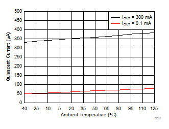
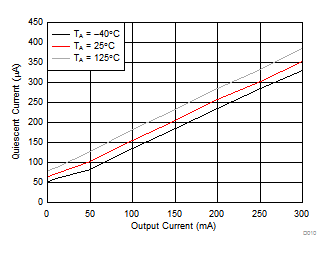
| 4 V ≤ VIN ≤ 40 V, IOUT < 100 µA, VADJ = 5 V | 60 | 100 | |||||
| 4 V ≤ VIN ≤ 40 V, IOUT < 300 mA, VADJ = 5V | 350 | 400 | |||||
| IQ(DROPOUT) | Current consumption in dropout region | VIN = VADJ = 5 V, IOUT = 100 µA | 70 | 140 | µA | ||
| II(ADJ) | Adjust input current | VADJ = VFB = 5 V | HTSSOP package | 0.5 | µA | ||
| SO PowerPAD package | 5.5 | ||||||
| V(ADJ_LOW) | Adjust low signal valid | VOUT = 0 V | HTSSOP package | 0 | 0.8 | V | |
| SO PowerPAD package | 0 | 0.7 | |||||
| V(ADJ_HIGH) | Adjust high signal valid | |VOUT – VADJ| < 4 mV | HTSSOP package | 1.5 | 18 | V | |
| SO PowerPAD package | 2 | 18 | |||||
| V(EN_LOW) | Enable low signal valid | VOUT = 0 V | 0 | 0.7 | V | ||
| V(EN_HIGH) | Enable high Signal Valid | OUT settled | 2 | 40 | V | ||
| IEN | Enable pulldown current | 2V < VEN < 40 V | 5 | µA | |||
| IFB | FB bias current | VADJ = VFB = 5 V | 0.5 | µA | |||
(1) The tracking accuracy is specified when the FB pin is directly connected to the OUT pin which means VADJ = VOUT, external resistor divider variance is not included.
(2) Measured when the output voltage, VOUT has dropped 10 mV from the nominal value.
6.6 Typical Characteristics
VIN = 14 V, VADJ = 5 V, VFB = VOUT, unless otherwise specified


| VIN = VADJ = 4 V | IOUT = 200 mA |


| C(OUT) = 10 µF | IOUT = 1 mA | TA = 25°C |

| VFB = VOUT | ||


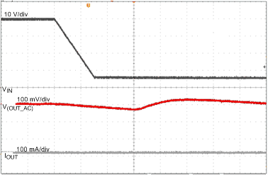
| VIN = 40 to 6 V | VADJ = 5 V | C(OUT) = 10 µF |
| IOUT = 100 mA, 20 µs/div | ||

| VIN = 40 to 6 V | VADJ = 5 V | C(OUT) = 10 µF |
| IOUT = 10 mA, 20 µs/div | ||

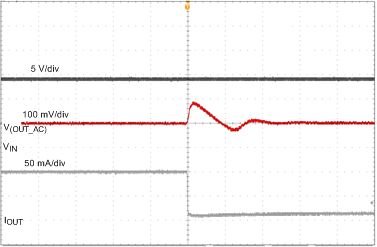
| VIN = 14 V | VADJ = 5 V | C(OUT) = 10 µF | ||
| IOUT = 100 to 10 mA, 40 µs/div | ||||


| VIN = VADJ = 4 V | ||


| VADJ = VEN = 5 V | ||

| C(OUT) = 10 µF | IOUT = 100 mA | TA = 25°C |

| VFB < VOUT | ||

| VIN = 6 to 40 V | VADJ = 5 V | C(OUT) = 10 µF |
| IOUT = 100 mA, 20 µs/div | ||

| VIN = 6 to 40 V | VADJ = 5 V | C(OUT) = 10 µF |
| IOUT = 10 mA, 20 µs/div | ||

| VIN = 14 V | VADJ = 5 V | C(OUT) = 10 µF |
| IOUT = 10 to 100 mA, 40 µs/div | ||