SBVS441 December   2022 TPS7B4255

PRODUCTION DATA  

  1. Features
  2. Applications
  3. Description
  4. Revision History
  5. Pin Configuration and Functions
  6. Specifications
    1. 6.1 Absolute Maximum Ratings
    2. 6.2 ESD Ratings
    3. 6.3 Recommended Operating Conditions
    4. 6.4 Thermal Information
    5. 6.5 Electrical Characteristics
    6.     Timing Characteristics
    7. 6.6 Typical Characteristics
  7. Detailed Description
    1. 7.1 Overview
    2. 7.2 Functional Block Diagram
    3. 7.3 Feature Description
      1. 7.3.1 Regulated Output (VOUT)
      2. 7.3.2 Undervoltage Lockout
      3. 7.3.3 Thermal Protection
      4. 7.3.4 Current Limit
      5. 7.3.5 VOUT Short to Battery
      6. 7.3.6 Tracking Regulator With an Enable Circuit
    4. 7.4 Device Functional Modes
      1. 7.4.1 Operation With VIN < 3 V
      2. 7.4.2 Operation With ADJ/EN Control
  8. Application and Implementation
    1. 8.1 Application Information
      1. 8.1.1 Dropout Voltage
      2. 8.1.2 Reverse Current
      3. 8.1.3 Signal-Buffering LDO
    2. 8.2 Typical Application
      1. 8.2.1 Design Requirements
      2. 8.2.2 Detailed Design Procedure
        1. 8.2.2.1 Input and Output Capacitor Selection
      3. 8.2.3 Application Curves
    3. 8.3 Power Supply Recommendations
    4. 8.4 Layout
      1. 8.4.1 Layout Guidelines
        1. 8.4.1.1 Package Mounting
        2. 8.4.1.2 Board Layout Recommendations to Improve PSRR and Noise Performance
        3. 8.4.1.3 Power Dissipation and Thermal Considerations
        4. 8.4.1.4 Thermal Performance Versus Copper Area
      2. 8.4.2 Layout Example
  9. Device and Documentation Support
    1. 9.1 Device Support
      1. 9.1.1 Device Nomenclature
      2. 9.1.2 Development Support
    2. 9.2 Receiving Notification of Documentation Updates
    3. 9.3 Support Resources
    4. 9.4 Trademarks
    5. 9.5 Electrostatic Discharge Caution
    6. 9.6 Glossary
  10. 10Mechanical, Packaging, and Orderable Information

Package Options

Mechanical Data (Package|Pins)
Thermal pad, mechanical data (Package|Pins)
Orderable Information

Typical Characteristics

VIN = VADJ/EN = 5 V, IOUT = 5 mA, 20 mA, 50 mA, 70 mA
Figure 6-1 Dropout Voltage vs Temperature
VIN = 13.5 V, VADJ/EN = 5 V
Figure 6-3 Ground Current vs Output Current
VIN = 13.5 V, VADJ/EN = 5 V
Figure 6-5 Current Limit vs Temperature
VADJ/EN = 5 V, IOUT = 10 mA
Figure 6-7 Output Voltage vs Input Voltage
VADJ/EN = 5 V, COUT = 10 μF, VIN = 9 V to 16 V
 
Figure 6-9 Line Transient
VIN = 13.5 V, COUT = 10 µF, IOUT = 1 mA, 10 mA, 50 mA, 70 mA, VADJ/EN = 5 V
Figure 6-11 Power-Supply Rejection Ratio vs Frequency
VIN = VADJ/EN = 5 V
Figure 6-2 Dropout Voltage vs Output Current
VIN = 13.5 V, VADJ/EN = 5 V
Figure 6-4 Ground Current vs Temperature
VIN = 13.5 V, VADJ/EN = 5 V
Figure 6-6 Tracking Error vs Temperature
VIN = 13.5 V, IOUT = 10 mA
Figure 6-8 Output Voltage vs Adjustable Voltage
VIN = 13.5 V, VADJ/EN = 5 V, COUT = 10 μF,
IOUT = 1 mA to 30 mA
Figure 6-10 Load Transient
GUID-20221121-SS0I-CM9V-FSBR-FDNBC3CZ8X54-low.png
 
 
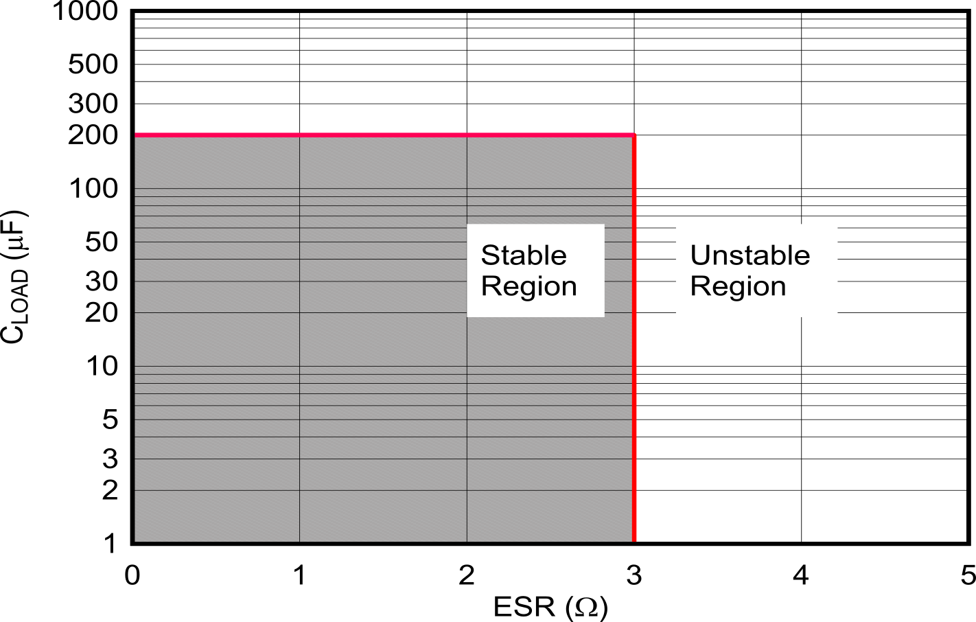
Figure 6-12 Load Capacitance vs ESR Stability