SLVSCE8C January   2015  – September 2018 TPS7B7701-Q1 , TPS7B7702-Q1

PRODUCTION DATA.  

  1. Features
  2. Applications
  3. Description
    1.     Application Diagram
  4. Revision History
  5. Pin Configuration and Functions
    1.     Pin Functions
  6. Specifications
    1. 6.1 Absolute Maximum Ratings
    2. 6.2 ESD Ratings
    3. 6.3 Recommended Operating Conditions
    4. 6.4 Thermal Information
    5. 6.5 Electrical Characteristics
    6. 6.6 Switching Characteristics
    7. 6.7 Typical Characteristics
  7. Detailed Description
    1. 7.1 Overview
    2. 7.2 Functional Block Diagram
    3. 7.3 Feature Description
      1. 7.3.1  Fault Detection and Protection
      2. 7.3.2  Short-Circuit and Overcurrent Protection
      3. 7.3.3  Short-to-Battery and Reverse Current Detection
      4. 7.3.4  Thermal Shutdown
      5. 7.3.5  Integrated Reverse-Polarity Protection
      6. 7.3.6  Integrated Inductive Clamp
      7. 7.3.7  Undervoltage Lockout
      8. 7.3.8  Enable (EN, EN1, and EN2)
      9. 7.3.9  Internal Voltage Regulator (VCC)
      10. 7.3.10 Current Sense Multiplexing
      11. 7.3.11 Adjustable Output Voltage (FB, FB1, and FB2)
    4. 7.4 Device Functional Modes
      1. 7.4.1 Operation With IN < 4.5 V
      2. 7.4.2 Operation With EN Control
  8. Application and Implementation
    1. 8.1 Application Information
    2. 8.2 Typical Application
      1. 8.2.1 Design Requirements
      2. 8.2.2 Detailed Design Procedure
        1. 8.2.2.1 Input Capacitor
        2. 8.2.2.2 Output Capacitor
        3. 8.2.2.3 Current Sense Resistor Selection
        4. 8.2.2.4 Current-Limit Resistor Selection
      3. 8.2.3 Application Curves
  9. Power Supply Recommendations
  10. 10Layout
    1. 10.1 Layout Guidelines
    2. 10.2 Layout Example
  11. 11Device and Documentation Support
    1. 11.1 Documentation Support
      1. 11.1.1 Related Documentation
    2. 11.2 Related Links
    3. 11.3 Receiving Notification of Documentation Updates
    4. 11.4 Community Resources
    5. 11.5 Trademarks
    6. 11.6 Electrostatic Discharge Caution
    7. 11.7 Glossary
  12. 12Mechanical, Packaging, and Orderable Information

Package Options

Refer to the PDF data sheet for device specific package drawings

Mechanical Data (Package|Pins)
  • PWP|16
Thermal pad, mechanical data (Package|Pins)
Orderable Information

Typical Characteristics

at VI = 14 V (unless otherwise specified)
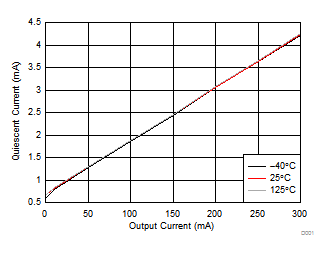
TPS7B7701-Q1 TPS7B7702-Q1 D001_slvsce8.gif
Figure 1. Quiescent Current vs Output Current
(TPS7B7702-Q1)
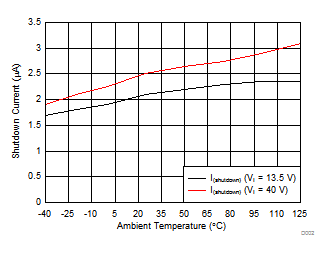
TPS7B7701-Q1 TPS7B7702-Q1 D002_slvsce8.gif
Figure 3. Shutdown Current vs Ambient Temperature (TPS7B7702-Q1)
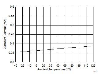
TPS7B7701-Q1 TPS7B7702-Q1 D013_slvsce8.gif
IO = 0.1 mA
Figure 5. Quiescent Current vs Ambient Temperature (TPS7B7701-Q1)
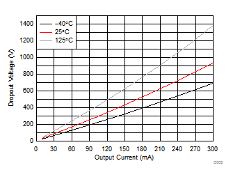
TPS7B7701-Q1 TPS7B7702-Q1 D005_slvsce8.gif
Figure 7. Dropout Voltage vs Output Current
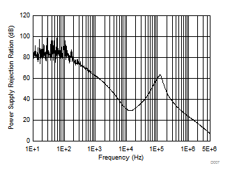
TPS7B7701-Q1 TPS7B7702-Q1 D007_slvsce8.gif
CO = 10 µF IO = 10 mA
Figure 9. PSRR TPS7B770x-Q1
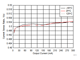
TPS7B7701-Q1 TPS7B7702-Q1 D010_slvsce8.gif
Figure 11. Current Sense Ratio vs Output Current, TPS7B7702-Q1 Channel 2
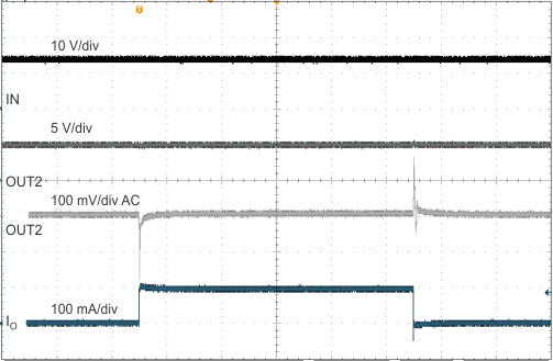
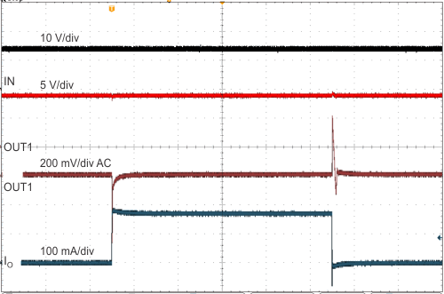
TPS7B7701-Q1 TPS7B7702-Q1 ac_load-transient_5_slvsce8.gif
VO = 5 V CO = 10 µF IO = 1 to 100 mA
Figure 13. 1-mA to 100-mA Load Transient
TPS7B7701-Q1 TPS7B7702-Q1 ac_line-transient_5_slvsce8.gif
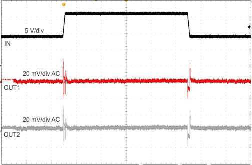
VO = 5 V IO = 50 mA
Figure 15. 9-V to 16-V Line Transient (1 V/µs)
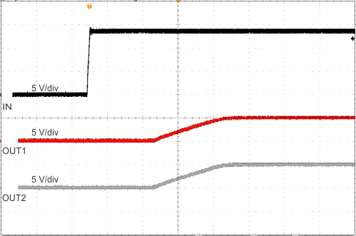
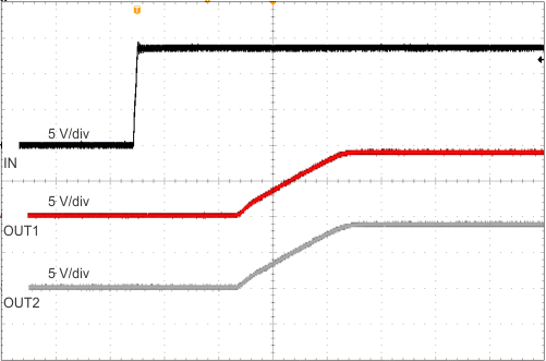
TPS7B7701-Q1 TPS7B7702-Q1 ac_powerup_5_slvsce8.gif
VO = 5 V IO = 100 mA VI = 0 to 14 V
Figure 17. Power Up (1 V/µs)
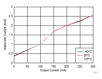
TPS7B7701-Q1 TPS7B7702-Q1 D012_slvsce8.gif
Figure 2. Quiescent Current vs Output Current
(TPS7B7701-Q1)
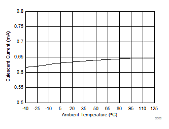
TPS7B7701-Q1 TPS7B7702-Q1 D003_slvsce8.gif
IO = 0.1 mA
Figure 4. Quiescent Current vs Ambient Temperature (TPS7B7702-Q1)
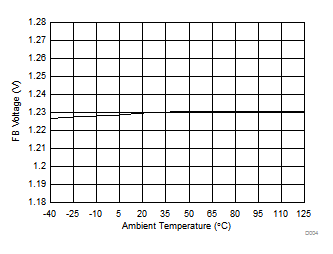
TPS7B7701-Q1 TPS7B7702-Q1 D004_slvsce8.gif
IO = 10 mA
Figure 6. FB Voltage vs Ambient Temperature
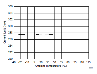
TPS7B7701-Q1 TPS7B7702-Q1 D006_slvsce8.gif
ILIM = 300 mA
Figure 8. Current Limit vs Ambient Temperature
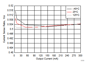
TPS7B7701-Q1 TPS7B7702-Q1 D009_slvsce8.gif
Figure 10. Current Sense Ratio vs Output Current, TPS7B7702-Q1 Channel 1
TPS7B7701-Q1 TPS7B7702-Q1 ac_load-transient_8p5_slvsce8.gif
VO = 8.5 V CO = 10 µF IO = 1 to 170 mA
Figure 12. 1-mA to 170-mA Load Transient
TPS7B7701-Q1 TPS7B7702-Q1 ac_line-transient_8p5_slvsce8.gif
VO = 8.5 V IO = 50 mA
Figure 14. 9-V to 16-V Line Transient (1 V/µs)
TPS7B7701-Q1 TPS7B7702-Q1 ac_powerup_8p5_slvsce8.gif
VO = 8.5 V IO = 100 mA VI = 0 to 14 V
Figure 16. Power Up (1 V/µs)
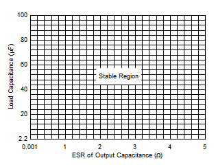
TPS7B7701-Q1 TPS7B7702-Q1 D011_slvsce8.gif
Figure 18. Load Capacitance vs ESR of Output Capacitance