SLVSCE8C January 2015 – September 2018 TPS7B7701-Q1 , TPS7B7702-Q1
PRODUCTION DATA.
- 1 Features
- 2 Applications
- 3 Description
- 4 Revision History
- 5 Pin Configuration and Functions
- 6 Specifications
-
7 Detailed Description
- 7.1 Overview
- 7.2 Functional Block Diagram
- 7.3
Feature Description
- 7.3.1 Fault Detection and Protection
- 7.3.2 Short-Circuit and Overcurrent Protection
- 7.3.3 Short-to-Battery and Reverse Current Detection
- 7.3.4 Thermal Shutdown
- 7.3.5 Integrated Reverse-Polarity Protection
- 7.3.6 Integrated Inductive Clamp
- 7.3.7 Undervoltage Lockout
- 7.3.8 Enable (EN, EN1, and EN2)
- 7.3.9 Internal Voltage Regulator (VCC)
- 7.3.10 Current Sense Multiplexing
- 7.3.11 Adjustable Output Voltage (FB, FB1, and FB2)
- 7.4 Device Functional Modes
- 8 Application and Implementation
- 9 Power Supply Recommendations
- 10Layout
- 11Device and Documentation Support
- 12Mechanical, Packaging, and Orderable Information
Package Options
Refer to the PDF data sheet for device specific package drawings
Mechanical Data (Package|Pins)
- PWP|16
Thermal pad, mechanical data (Package|Pins)
- PWP|16
Orderable Information
3 Description
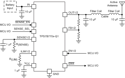
The TPS7B770x-Q1 family of devices feature a single and dual, high-voltage low-dropout regulator (LDO) with current sensing, designed to operate with a wide input-voltage range from 4.5 V to 40 V (45-V load dump protection). These devices provide power to the low-noise amplifiers of the active antenna through a coax cable with 300 mA per channel current. Each channel also provides an adjustable output voltage from 1.5 V to 20 V.
These devices provide diagnostics through the current sense and error pins. To monitor the load current, a high-side current-sense circuitry provides a proportional analog output to the sensed load current. The accurate current sense allows detection of open, normal, and short-circuit conditions without the need for further calibration. Current sense can be multiplexed between channels and devices to save analog-to-digital converter (ADC) resources. Each channel also implements adjustable current limit with an external resistor.
An integrated reverse polarity diode eliminates the need for an external diode. These devices feature standard thermal shutdown, short-to-battery protection on the output, and reverse current protection. Each channel has internal inductive clamp protection on the output during inductive switch off.
These devices operate over a –40°C to +125°C ambient temperature range.
Device Information(1)
| PART NUMBER | PACKAGE | CHANNEL |
|---|---|---|
| TPS7B7701-Q1 | HTSSOP (16) | Single |
| TPS7B7702-Q1 | HTSSOP (16) | Dual |
- For all available packages, see the package option addendum at the end of the data sheet.
Application Diagram
