SBVS361A April 2020 – November 2020 TPS7B84-Q1
PRODUCTION DATA
- 1 Features
- 2 Applications
- 3 Description
- 4 Revision History
- 5 Pin Configuration and Functions
- 6 Specifications
- 7 Detailed Description
- 8 Application and Implementation
- 9 Power Supply Recommendations
- 10Layout
- 11Device and Documentation Support
Package Options
Refer to the PDF data sheet for device specific package drawings
Mechanical Data (Package|Pins)
- DCY|4
- DRB|8
Thermal pad, mechanical data (Package|Pins)
- DRB|8
Orderable Information
3 Description
The TPS7B84-Q1 is a low-dropout linear
regulator designed to connect to the battery in automotive applications. The device
has an input voltage range extending to 40 V, which allows the device to withstand
transients (such as load dump) that are anticipated in automotive systems. With only
an
18-µA quiescent current, the device is an optimal
solution for powering always-on components such as microcontrollers (MCUs) and
controller area network (CAN) transceivers in standby systems.
The TPS7B84-Q1 has both fixed and adjustable output types. The wide output voltage range allows the device to generate the bias voltage for silicon carbide (SiC) gate drivers and microphones as well as power MCUs and processors.
The device has state-of-the-art transient response that allows the output to quickly react to changes in load or line (for example, during cold-crank conditions). Additionally, the device has a novel architecture that minimizes output overshoot when recovering from dropout. During normal operation, the device has a tight DC accuracy of ±0.75% over line, load, and temperature.
The device is available in both a SOT223 package and a small VSON package with wettable flanks that facilitates a compact printed circuit board (PCB) design. The low thermal resistance enables sustained operation despite significant dissipation across the device.
| PART NUMBER | PACKAGE | BODY SIZE (NOM) |
|---|---|---|
| TPS7B84-Q1 | VSON (8) | 3.00 mm × 3.00 mm |
| SOT-223 (4) | 6.50 mm × 3.50 mm |
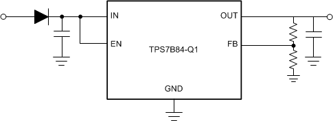
 Typical Application Schematic