SBVS361A April   2020  – November 2020 TPS7B84-Q1

PRODUCTION DATA  

  1. Features
  2. Applications
  3. Description
  4. Revision History
  5. Pin Configuration and Functions
  6. Specifications
    1. 6.1 Absolute Maximum Ratings
    2. 6.2 ESD Ratings
    3. 6.3 Recommended Operating Conditions
    4. 6.4 Thermal Information
    5. 6.5 Electrical Characteristics
    6. 6.6 Typical Characteristics
  7. Detailed Description
    1. 7.1 Overview
    2. 7.2 Functional Block Diagrams
    3. 7.3 Feature Description
      1. 7.3.1 Enable (EN)
      2. 7.3.2 Undervoltage Lockout
      3. 7.3.3 Thermal Shutdown
      4. 7.3.4 Current Limit
    4. 7.4 Device Functional Modes
      1. 7.4.1 Device Functional Mode Comparison
      2. 7.4.2 Normal Operation
      3. 7.4.3 Dropout Operation
      4. 7.4.4 Disabled
  8. Application and Implementation
    1. 8.1 Application Information
      1. 8.1.1 Input and Output Capacitor Selection
      2. 8.1.2 Adjustable Device Feedback Resistor Selection
      3. 8.1.3 Feed-Forward Capacitor (CFF)
      4. 8.1.4 Dropout Voltage
      5. 8.1.5 Reverse Current
      6. 8.1.6 Power Dissipation (PD)
        1. 8.1.6.1 Thermal Performance Versus Copper Area
        2. 8.1.6.2 Power Dissipation vs Ambient Temperature
      7. 8.1.7 Estimating Junction Temperature
    2. 8.2 Typical Application
      1. 8.2.1 Design Requirements
      2. 8.2.2 Detailed Design Procedure
        1. 8.2.2.1 Input Capacitor
        2. 8.2.2.2 Output Capacitor
      3. 8.2.3 Application Curves
  9. Power Supply Recommendations
  10. 10Layout
    1. 10.1 Layout Guidelines
      1. 10.1.1 Package Mounting
      2. 10.1.2 Board Layout Recommendations to Improve PSRR and Noise Performance
    2. 10.2 Layout Examples
  11. 11Device and Documentation Support
    1. 11.1 Device Support
      1. 11.1.1 Device Nomenclature
    2. 11.2 Receiving Notification of Documentation Updates
    3. 11.3 Support Resources
    4. 11.4 Trademarks
    5. 11.5 Electrostatic Discharge Caution
    6. 11.6 Glossary

Package Options

Refer to the PDF data sheet for device specific package drawings

Mechanical Data (Package|Pins)
  • DCY|4
  • DRB|8
Thermal pad, mechanical data (Package|Pins)
Orderable Information

Applications


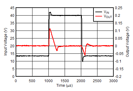
GUID-07A57807-C8BC-4CF4-8BB4-DCB689CDEAE1-low.gif Line Transient Response (3-V/µs VIN Slew Rate)