SBVS360A February   2020  – November 2020 TPS7B85-Q1

PRODUCTION DATA  

  1. Features
  2. Applications
  3. Description
  4. Revision History
  5. Pin Configuration and Functions
  6. Specifications
    1. 6.1 Absolute Maximum Ratings
    2. 6.2 ESD Ratings
    3. 6.3 Recommended Operating Conditions
    4. 6.4 Thermal Information
    5. 6.5 Electrical Characteristics
    6. 6.6 Switching Characteristics
    7. 6.7 Typical Characteristics
  7. Detailed Description
    1. 7.1 Overview
    2. 7.2 Functional Block Diagram
    3. 7.3 Feature Description
      1. 7.3.1 Enable (EN)
      2. 7.3.2 Power-Good (PG)
        1. 7.3.2.1 Adjustable Power-Good (PGADJ)
      3. 7.3.3 Adjustable Power-Good Delay Timer (DELAY)
      4. 7.3.4 Sense Comparator
      5. 7.3.5 Undervoltage Lockout
      6. 7.3.6 Thermal Shutdown
      7. 7.3.7 Current Limit
    4. 7.4 Device Functional Modes
      1. 7.4.1 Device Functional Mode Comparison
      2. 7.4.2 Normal Operation
      3. 7.4.3 Dropout Operation
      4. 7.4.4 Disabled
  8. Application and Implementation
    1. 8.1 Application Information
      1. 8.1.1 Input and Output Capacitor Selection
      2. 8.1.2 Dropout Voltage
      3. 8.1.3 Reverse Current
      4. 8.1.4 Power Dissipation (PD)
        1. 8.1.4.1 Thermal Performance Versus Copper Area
      5. 8.1.5 Estimating Junction Temperature
      6. 8.1.6 SI Pin
        1. 8.1.6.1 Calculating the Sense Input (SI) Pin Threshold
        2. 8.1.6.2 Different Uses for the Sense Input Pin
          1. 8.1.6.2.1 Monitoring Input Voltage
          2. 8.1.6.2.2 Creating OV and UV Power-Good
          3. 8.1.6.2.3 Monitoring a Separate Supply Voltage
      7. 8.1.7 Pulling Up the SO and PG Pins to a Different Voltage
      8. 8.1.8 Power-Good
        1. 8.1.8.1 Setting the Adjustable Power-Good Threshold
        2. 8.1.8.2 Setting the Adjustable Power-Good Delay
    2. 8.2 Typical Application
      1. 8.2.1 Design Requirements
      2. 8.2.2 Detailed Design Procedure
        1. 8.2.2.1 Input Capacitor
        2. 8.2.2.2 Output Capacitor
      3. 8.2.3 Application Curves
  9. Power Supply Recommendations
  10. 10Layout
    1. 10.1 Layout Guidelines
      1. 10.1.1 Package Mounting
      2. 10.1.2 Board Layout Recommendations to Improve PSRR and Noise Performance
    2. 10.2 Layout Example
  11. 11Device and Documentation Support
    1. 11.1 Device Support
      1. 11.1.1 Device Nomenclature
    2. 11.2 Receiving Notification of Documentation Updates
    3. 11.3 Support Resources
    4. 11.4 Trademarks
    5. 11.5 Electrostatic Discharge Caution
    6. 11.6 Glossary

Package Options

Mechanical Data (Package|Pins)
Thermal pad, mechanical data (Package|Pins)
Orderable Information
Creating OV and UV Power-Good

Another feature that is often desired is the ability to monitor the output voltage for overvoltage (OV) or undervoltage (UV) events. Because the integrated power-good pin only detects undervoltage events, a separate solution must be implemented to monitor for overvoltage issues. This monitoring can be done by using the integrated SI pin and connecting this pin to the output through a resistor divider. Then place the rising threshold of the SI pin where the output voltage is going to be flagged as overvoltage. Equation 7 depicts how to calculate the resistor divider for this application based on the desired overvoltage threshold. If this method is used for creating an overvoltage detection, the output of the overvoltage signal has inverted logic. Figure 8-8 shows the typical configuration for using the device as an overvotlage monitor.

Equation 7. GUID-DB021863-D583-4A97-913F-2086FA72D027-low.gif
GUID-66B8CF5B-F01C-4979-B64F-F7BC417CB325-low.gif
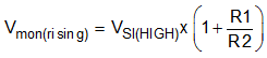
Figure 8-8 Creating an Overvoltage Detector on the Output