SBVS360A February 2020 – November 2020 TPS7B85-Q1
PRODUCTION DATA
- 1 Features
- 2 Applications
- 3 Description
- 4 Revision History
- 5 Pin Configuration and Functions
- 6 Specifications
- 7 Detailed Description
- 8 Application and Implementation
- 9 Power Supply Recommendations
- 10Layout
- 11Device and Documentation Support
Package Options
Mechanical Data (Package|Pins)
- DRC|10
Thermal pad, mechanical data (Package|Pins)
- DRC|10
Orderable Information
5 Pin Configuration and Functions
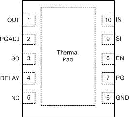
 Figure 5-1 DRC
Package,10-Pin VSON,Top View
Figure 5-1 DRC
Package,10-Pin VSON,Top ViewTable 5-1 Pin Functions
| PIN | TYPE(1) | DESCRIPTION | |
|---|---|---|---|
| NAME | DRC | ||
| DELAY | 4 | O | Power-good delay adjustment pin. Connect a capacitor from this pin to GND to set the PG reset delay. Leave this pin floating for a default (t(DLY_FIX)) delay. See the Section 8.1.8 section for more information. If this functionality is not desired, leave this pin floating because connecting this pin to GND causes a perminant increase in the GND current. |
| EN | 8 | I | Enable pin. The device is disabled when the enable pin becomes lower than the enable logic input low level (VIL). To ensure the device is enabled, the EN pin must be driven above the logic high level (VIH). This pin should not be left floating as this pin is high impedance if it is left floating the part may enable or disable. |
| GND | 6 | G | Ground pin. Connect this pin to the thermal pad with a low-impedance connection. |
| NC | 5 | — | No internal connection. Connect this pin to GND for the best thermal resistance. |
| PGADJ | 2 | I | Power-good threshold-adjustment pin. Connect a resistor divider between the PGADJ and OUT pins to set the power-good threshold. Connect this pin to ground to set the threshold to VPG(TH,FALLING). See Section 8.1.8 for more information. |
| PG | 7 | O | Power-good pin. This pin has an internal pullup resistor. Do not connect this pin to VOUT or any other biased voltage rail. VPG is logic level high when VOUT is above the power-good threshold. See Section 8.1.8 for more information. |
| SI | 9 | I | Sense input pin. Connect via an external voltage divider to the supply voltage to be monitored. |
| SO | 3 | O | Sense output pin. This pin has an internal pullup resistor. Do not connect this pin to VOUT or any other biased voltage rail. VSO is logic level low when VSI falls below the sense-low threshold. |
| IN | 10 | P | Input power-supply voltage pin. For best transient response and to minimize input impedance, use the recommended value or larger ceramic capacitor from IN to ground as listed in the Recommended Operating Conditions table and the Section 8.2.2.1 section. Place the input capacitor as close to the input of the device as possible. |
| OUT | 1 | O | Regulated output voltage pin. A capacitor is required from OUT to ground for stability. For best transient response, use the nominal recommended value or larger ceramic capacitor from OUT to ground; see the Recommended Operating Conditions table and the Section 8.2.2.2 section. Place the output capacitor as close to the output of the device as possible. If using a high ESR capacitor, decouple the output with a 100-nF ceramic capacitor. |
| Thermal pad | — | Thermal pad. Connect the pad to GND for the best possible thermal performance. See the Section 10 section for more information. | |
(1) I = input; O = output; P = power; G = ground.