SBVS360A February 2020 – November 2020 TPS7B85-Q1
PRODUCTION DATA
- 1 Features
- 2 Applications
- 3 Description
- 4 Revision History
- 5 Pin Configuration and Functions
- 6 Specifications
- 7 Detailed Description
- 8 Application and Implementation
- 9 Power Supply Recommendations
- 10Layout
- 11Device and Documentation Support
Package Options
Mechanical Data (Package|Pins)
- DRC|10
Thermal pad, mechanical data (Package|Pins)
- DRC|10
Orderable Information
8.1.8.1 Setting the Adjustable Power-Good Threshold
The power-good threshold is also adjustable from 1 V to 18 V with an external resistor divider between PGADJ and OUT. Use Equation 8 to calculate this threshold:
Equation 8. 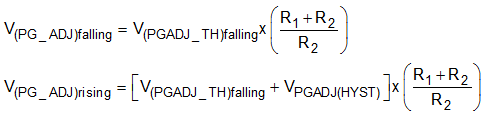
where
- V(PG_ADJ) rising, V(PG_ADJ) falling is the adjustable power-good threshold
- V(PGADJ_TH) falling is the internal comparator reference voltage of the PGADJ pin
By setting the power-good threshold V(PG_ADJ) rising, when VOUT exceeds this threshold, the PG output turns high after the power-good delay period has expired. When VOUT falls below V(PG_ADJ) falling, the PG output turns low after a short deglitch time. Figure 8-11 shows a diagram of the PG threshold.
 Figure 8-11 Adjustable Power-Good Threshold