SBVS363A December   2020  – April 2021 TPS7B87-Q1

PRODUCTION DATA  

  1. Features
  2. Applications
  3. Description
  4. Revision History
  5. Pin Configuration and Functions
  6. Specifications
    1. 6.1 Absolute Maximum Ratings
    2. 6.2 ESD Ratings
    3. 6.3 Recommended Operating Conditions
    4. 6.4 Thermal Information
    5. 6.5 Electrical Characteristics
    6. 6.6 Switching Characteristics
    7. 6.7 Typical Characteristics
  7. Detailed Description
    1. 7.1 Overview
    2. 7.2 Functional Block Diagram
    3. 7.3 Feature Description
      1. 7.3.1 Power-Good (PG)
      2. 7.3.2 Adjustable Power-Good Delay Timer (DELAY)
      3. 7.3.3 Undervoltage Lockout
      4. 7.3.4 Thermal Shutdown
      5. 7.3.5 Current Limit
    4. 7.4 Device Functional Modes
      1. 7.4.1 Device Functional Mode Comparison
      2. 7.4.2 Normal Operation
      3. 7.4.3 Dropout Operation
      4. 7.4.4 Disabled
  8. Application and Implementation
    1. 8.1 Application Information
      1. 8.1.1 Input and Output Capacitor Selection
      2. 8.1.2 Dropout Voltage
      3. 8.1.3 Reverse Current
      4. 8.1.4 Power Dissipation (PD)
        1. 8.1.4.1 Thermal Performance Versus Copper Area
        2. 8.1.4.2 Power Dissipation Versus Ambient Temperature
      5. 8.1.5 Estimating Junction Temperature
      6. 8.1.6 Pulling Up the PG Pin to a Different Voltage
      7. 8.1.7 Power-Good
        1. 8.1.7.1 Setting the Adjustable Power-Good Delay
    2. 8.2 Typical Application
      1. 8.2.1 Design Requirements
      2. 8.2.2 Detailed Design Procedure
        1. 8.2.2.1 Input Capacitor
        2. 8.2.2.2 Output Capacitor
      3. 8.2.3 Application Curves
  9. Power Supply Recommendations
  10. 10Layout
    1. 10.1 Layout Guidelines
      1. 10.1.1 Package Mounting
      2. 10.1.2 Board Layout Recommendations to Improve PSRR and Noise Performance
    2. 10.2 Layout Examples
  11. 11Device and Documentation Support
    1. 11.1 Device Support
      1. 11.1.1 Device Nomenclature
      2. 11.1.2 Development Support
    2. 11.2 Documentation Support
      1. 11.2.1 Related Documentation
    3. 11.3 Receiving Notification of Documentation Updates
    4. 11.4 Support Resources
    5. 11.5 Trademarks
    6. 11.6 Electrostatic Discharge Caution
    7. 11.7 Glossary
  12. 12Mechanical, Packaging, and Orderable Information

Package Options

Mechanical Data (Package|Pins)
Thermal pad, mechanical data (Package|Pins)
Orderable Information

Power-Good (PG)

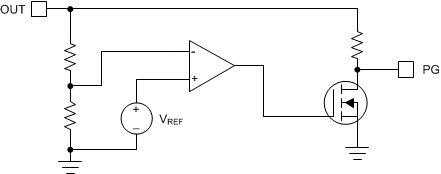
The PG signal provides an easy solution to meet demanding sequencing requirements because PG alerts when the output nears its nominal value. PG can be used to signal other devices in a system when the output voltage is near, at, or above the set output voltage (VOUT(nom)). Figure 7-1 shows a simplified schematic. The PG signal is an internal pullup resistor to the nominal output voltage and is active high. The PG circuit sets the PG pin into a high-impedance state to indicate that the power is good.
GUID-803FEA5D-1014-4685-B25A-603C54B0F050-low.gifFigure 7-1 Simplified Power-Good Schematic