SLVSAS4J June   2013  – April 2017 TPS7H1201-HT

PRODUCTION DATA.  

  1. Features
  2. Applications
  3. Description
  4. Revision History
  5. Pin Configuration and Functions
  6. Specifications
    1. 6.1 Absolute Maximum Ratings
    2. 6.2 ESD Ratings
    3. 6.3 Recommended Operating Conditions
    4. 6.4 Thermal Information
    5. 6.5 Electrical Characteristics
    6. 6.6 Typical Characteristics
  7. Detailed Description
    1. 7.1 Overview
    2. 7.2 Functional Block Diagram
    3. 7.3 Feature Description
      1. 7.3.1 Soft Start
      2. 7.3.2 Power Good (PG)
    4. 7.4 Device Functional Modes
      1. 7.4.1 Enable/Disable
  8. Application and Implementation
    1. 8.1 Application Information
      1. 8.1.1 Stability
    2. 8.2 Typical Application
      1. 8.2.1 Design Requirements
      2. 8.2.2 Detailed Design Procedure
        1. 8.2.2.1 Adjustable Output Voltage (Feedback Circuit)
        2. 8.2.2.2 PCL
        3. 8.2.2.3 High-Side Current Sense
        4. 8.2.2.4 Current Foldback
        5. 8.2.2.5 Transient Response
        6. 8.2.2.6 Current Sharing
        7. 8.2.2.7 Compensation
        8. 8.2.2.8 Output Noise
        9. 8.2.2.9 Capacitors
      3. 8.2.3 Application Curves
  9. Power Supply Recommendations
  10. 10Layout
    1. 10.1 Layout Guidelines
    2. 10.2 Layout Example
  11. 11Device and Documentation Support
    1. 11.1 Device Support
      1. 11.1.1 Third-Party Products Disclaimer
      2. 11.1.2 Device Nomenclature
    2. 11.2 Documentation Support
      1. 11.2.1 Related Documentation
    3. 11.3 Receiving Notification of Documentation Updates
    4. 11.4 Community Resources
    5. 11.5 Trademarks
    6. 11.6 Electrostatic Discharge Caution
    7. 11.7 Glossary
  12. 12Mechanical, Packaging, and Orderable Information

Package Options

Mechanical Data (Package|Pins)
Thermal pad, mechanical data (Package|Pins)
Orderable Information

Layout

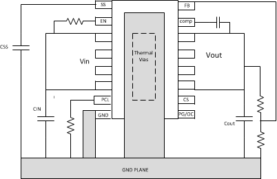
Layout Guidelines

  • For best performance, all traces should be as short as possible, and no longer than 5 cm.
  • Use wide traces for IN, Out and GND to minimize the parasitic electrical effects.
  • Place the output capacitors (COUT) as close as possible to the OUT pin of the device.

Layout Example

TPS7H1201-HT layout_ex_LVSAS4.gif Figure 30. PCB Layout Example