SLVSCJ5C December 2015 – September 2024 TPS7H3301-SP
PRODUCTION DATA
- 1
- 1 Features
- 2 Applications
- 3 Description
- 4 Revision History
- 5 Pin Configuration and Functions
- 6 Specifications
- 7 Detailed Description
-
8 Application and Implementation
- 8.1 Application Information
- 8.2
Typical Application
- 8.2.1 Design Requirements
- 8.2.2
Detailed Design Procedure
- 8.2.2.1 VDD/VIN Capacitor
- 8.2.2.2 VLDO Input Capacitor
- 8.2.2.3 VTT Output Capacitor
- 8.2.2.4 VTTSNS Connection
- 8.2.2.5 Low VIN Applications
- 8.2.2.6 S3 and Pseudo-S5 Support
- 8.2.2.7 Tracking Startup and Shutdown
- 8.2.2.8 Output Tolerance Consideration for VTT DIMM or Module Applications
- 8.2.2.9 LDO Design Guidelines
- 8.2.3 Application Curve
- Power Supply Recommendations
- 9 Layout
- 10Device and Documentation Support
- Mechanical, Packaging, and Orderable Information
Package Options
Mechanical Data (Package|Pins)
- HKR|16
Thermal pad, mechanical data (Package|Pins)
Orderable Information
8.2.2.7 Tracking Startup and Shutdown
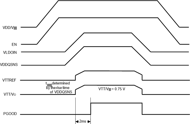
The TPS7H3301-SP supports tracking startup of VDDQ and shutdown when EN is tied directly to the system bus and not used to turn on or turn off the device. During tracking startup, VTT/VO follows VTTREF once VDDQSNS voltage is greater than 0.78 V. VDDQSNS incorporates a resistor divider network and a time constant of about 445 µs. The rise time of the VTT/VO output is then a function of the rise time of VDDQSNS. If the VDDQSNS rise time is larger than 445 µs. PGOOD is asserted 2 ms after VTT/VO is within ±20% of VTTREF. During tracking shutdown, VTT/VO falls following VTTREF until VTTREF reaches 0.37 V. Once VTTREF falls below 0.37 V, the internal discharge MOSFETs are turned on and quickly discharge both VTTREF and VTT/VO to GND. PGOOD is deasserted once VTT/VO is beyond the ±20% range of VTTREF. Figure 8-4 shows the typical timing diagram for an application that uses tracking startup and shutdown.
There are no sequencing requirements between VDD/VIN and VLDOIN. If VLDOIN is applied first followed by VDD/VIN there is no issue. VDD/VIN UVLO protection monitors VDD/VIN voltage. When VDD/VIN is lower than UVLO threshold both VTT and VTTREF regulators are powered off.
 Figure 8-4 Typical Timing Diagram of Tracking Startup and Shutdown