SLVSCJ5C December   2015  – September 2024 TPS7H3301-SP

PRODUCTION DATA  

  1.   1
  2. Features
  3. Applications
  4. Description
  5. Revision History
  6. Pin Configuration and Functions
  7. Specifications
    1. 6.1 Absolute Maximum Ratings
    2. 6.2 ESD Ratings
    3. 6.3 Recommended Operating Conditions
    4. 6.4 Thermal Information
    5. 6.5 Electrical Characteristics
    6. 6.6 Typical Characteristics
  8. Detailed Description
    1. 7.1 Overview
    2. 7.2 Functional Block Diagram
    3. 7.3 Feature Description
      1. 7.3.1 VTT/VO Sink and Source Regulator
      2. 7.3.2 Reference Input (VDDQSNS)
      3. 7.3.3 Reference Output (VTTREF)
      4. 7.3.4 EN Control (EN)
      5. 7.3.5 Power-Good Function (PGOOD)
      6. 7.3.6 VTT Current Protection
      7. 7.3.7 VIN UVLO Protection
      8. 7.3.8 Thermal Shutdown
    4. 7.4 Device Functional Modes
  9. Application and Implementation
    1. 8.1 Application Information
    2. 8.2 Typical Application
      1. 8.2.1 Design Requirements
      2. 8.2.2 Detailed Design Procedure
        1. 8.2.2.1 VDD/VIN Capacitor
        2. 8.2.2.2 VLDO Input Capacitor
        3. 8.2.2.3 VTT Output Capacitor
        4. 8.2.2.4 VTTSNS Connection
        5. 8.2.2.5 Low VIN Applications
        6. 8.2.2.6 S3 and Pseudo-S5 Support
        7. 8.2.2.7 Tracking Startup and Shutdown
        8. 8.2.2.8 Output Tolerance Consideration for VTT DIMM or Module Applications
        9. 8.2.2.9 LDO Design Guidelines
      3. 8.2.3 Application Curve
  10.   Power Supply Recommendations
  11. Layout
    1. 9.1 Layout Guidelines
    2. 9.2 Layout Example
    3. 9.3 Thermal Considerations
  12. 10Device and Documentation Support
    1. 10.1 Device Support
      1. 10.1.1 Third-Party Products Disclaimer
    2. 10.2 Documentation Support
      1. 10.2.1 Related Documentation
    3. 10.3 Receiving Notification of Documentation Updates
    4. 10.4 Support Resources
    5. 10.5 Trademarks
    6. 10.6 Electrostatic Discharge Caution
    7. 10.7 Glossary
  13.   Mechanical, Packaging, and Orderable Information

Package Options

Mechanical Data (Package|Pins)
Thermal pad, mechanical data (Package|Pins)
Orderable Information

Typical Application

The design example describes a 2.5-V VIN, DDR3 configuration.
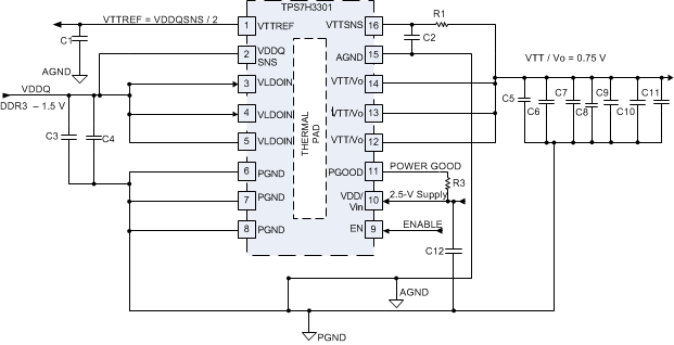
TPS7H3301-SP Typical Application CircuitFigure 8-1 Typical Application Circuit