SLVSCJ5C December 2015 – September 2024 TPS7H3301-SP
PRODUCTION DATA
- 1
- 1 Features
- 2 Applications
- 3 Description
- 4 Revision History
- 5 Pin Configuration and Functions
- 6 Specifications
- 7 Detailed Description
-
8 Application and Implementation
- 8.1 Application Information
- 8.2
Typical Application
- 8.2.1 Design Requirements
- 8.2.2
Detailed Design Procedure
- 8.2.2.1 VDD/VIN Capacitor
- 8.2.2.2 VLDO Input Capacitor
- 8.2.2.3 VTT Output Capacitor
- 8.2.2.4 VTTSNS Connection
- 8.2.2.5 Low VIN Applications
- 8.2.2.6 S3 and Pseudo-S5 Support
- 8.2.2.7 Tracking Startup and Shutdown
- 8.2.2.8 Output Tolerance Consideration for VTT DIMM or Module Applications
- 8.2.2.9 LDO Design Guidelines
- 8.2.3 Application Curve
- Power Supply Recommendations
- 9 Layout
- 10Device and Documentation Support
- Mechanical, Packaging, and Orderable Information
Package Options
Mechanical Data (Package|Pins)
- HKR|16
Thermal pad, mechanical data (Package|Pins)
Orderable Information
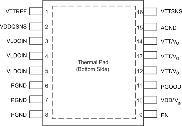
5 Pin Configuration and Functions
 Figure 5-1 HKR
Package,16-Pin CFP(Top View)
Figure 5-1 HKR
Package,16-Pin CFP(Top View)Table 5-1 Pin Functions
| PIN | I/O | DESCRIPTION | |
|---|---|---|---|
| NAME | NO. | ||
| VTTREF | 1 | O | Reference output. Connect to GND through 0.1-µF ceramic capacitor. |
| VDDQSNS | 2 | I | VDDQ sense input. Reference input for VTTREF. |
| VLDOIN | 3 | I | Supply voltage for the LDO. Connect to VDDQ voltage or an alternate voltage source. |
| 4 | |||
| 5 | |||
| PGND | 6 | — | Power ground. Connect output for the VTT/VO LDO to negative pin of the output capacitor. |
| 7 | |||
| 8 | |||
| EN | 9 | I | Enable pin. Driving this pin to logic high enables the device; driving this pin to logic low disables the device. |
| VDD/VIN | 10 | I | 2.5- or 3.3-V power supply. A ceramic decoupling capacitor with a value between 1 and 10 µF is required. |
| PGOOD | 11 | O | PGOOD output pin. PGOOD pin is an open drain output to indicate the output voltage is within specification. |
| VTT/VO | 12 | O | Power output for VTT/VO LDO. |
| 13 | |||
| 14 | |||
| AGND | 15 | — | Signal ground. Connect to negative pin of output capacitors.(1) |
| VTTSNS | 16 | I | Voltage sense for VTT/VO. Connect to positive pin of the output capacitor or the load. |
(1) Thermal pad and package lid are internally connected to ground.