SLVSGX6B February 2023 – December 2023 TPS7H3302-SEP , TPS7H3302-SP
PRODUCTION DATA
- 1
- 1 Features
- 2 Applications
- 3 Description
- 4 Device Options
- 5 Pin Configuration and Functions
- 6 Specifications
- 7 Detailed Description
-
8 Application and Implementation
- 8.1 Application Information
- 8.2
Typical Application
- 8.2.1 Design Requirements
- 8.2.2
Detailed Design Procedure
- 8.2.2.1 VDD Capacitor
- 8.2.2.2 VLDO Input Capacitor
- 8.2.2.3 VTT Output Capacitor
- 8.2.2.4 VTTSNS Connection
- 8.2.2.5 Low VDD Applications
- 8.2.2.6 S3 and Pseudo-S5 Support
- 8.2.2.7 Tracking Startup and Shutdown
- 8.2.2.8 Output Tolerance Consideration for VTT DIMM or Module Applications
- 8.2.2.9 LDO Design Guidelines
- 8.2.3 Application Curve
- 8.3 Power Supply Recommendations
- 8.4 Layout
- 9 Device and Documentation Support
- 10Revision History
- 11Mechanical, Packaging, and Orderable Information
Package Options
Refer to the PDF data sheet for device specific package drawings
Mechanical Data (Package|Pins)
- DAP|32
Thermal pad, mechanical data (Package|Pins)
- DAP|32
Orderable Information
5 Pin Configuration and Functions
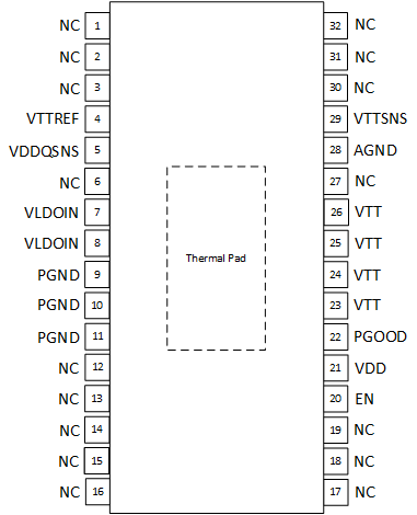
 Figure 5-1 DAP
Package, 32-Pin HTSSOP (Top View)
Figure 5-1 DAP
Package, 32-Pin HTSSOP (Top View)Pin Functions
| PIN | I/O(1) | DESCRIPTION | |
|---|---|---|---|
| NAME | NO. | ||
| VTTREF | 4 | O | Reference output. Connect to GND through 0.1-µF ceramic capacitor. |
| VDDQSNS | 5 | I | VDDQ sense input. Reference input for VTTREF.(2) |
| VLDOIN | 7 | I | Supply voltage for the LDO. Connect to VDDQ voltage or an alternate voltage source. |
| 8 | |||
| PGND | 9 | — | Power ground. Connect to system ground. |
| 10 | |||
| 11 | |||
| EN | 20 | I | Enable pin. Driving this pin to logic high enables the device; driving this pin to logic low disables the device. |
| VDD | 21 | I | 2.5- or 3.3-V power supply. A ceramic decoupling capacitor with a value between 1 and 10 µF is required. |
| PGOOD | 22 | O | PGOOD output pin. PGOOD pin is an open drain output to indicate the output voltage is within specification. |
| VTT | 23 | O | Power output for VTT LDO. |
| 24 | |||
| 25 | |||
| 26 | |||
| AGND | 28 | — | Signal ground. Connect to system ground. |
| VTTSNS | 29 | I | Voltage sense for VTT. Place capacitor close to pin. Route sense line to VTT near load. |
| NC | 1-3, 6, 12-19, 27, 30-32 | — | No connect. These pins are not internally connected. It is recommended to connect these pins to ground to prevent charge buildup; however, these pins can also be left open or tied to any voltage between ground and VDD. |
| Thermal Pad | — | Connect to PGND. This is internally floating. | |
(1) I = Input, O = Output, — = Other
(2) VDDQSNS shall be connected to the
regulated voltage supplying VDDQ. If the VDDQ supply is also used for VLDOIN, an RC filter
is recommended to isolate transients from VLDOIN to VDDQ.