SNVS983A April 2024 – August 2024 TPS7H4011-SP
PRODMIX
- 1
- 1 Features
- 2 Applications
- 3 Description
- 4 Device Options Table
- 5 Pin Configuration and Functions
- 6 Specifications
- 7 Parameter Measurement Information
-
8 Detailed Description
- 8.1 Overview
- 8.2 Functional Block Diagram
- 8.3
Feature Description
- 8.3.1 VIN and Power VIN Pins (VIN and PVIN)
- 8.3.2 Voltage Reference
- 8.3.3 Remote Sensing and Setting VOUT
- 8.3.4 Enable
- 8.3.5 Fault Input (FAULT)
- 8.3.6 Power Good (PWRGD)
- 8.3.7 Adjustable Switching Frequency and Synchronization
- 8.3.8 Turn-On Behavior
- 8.3.9 Protection Modes
- 8.3.10 Error Amplifier and Loop Response
- 8.4 Device Functional Modes
-
9 Application and Implementation
- 9.1 Application Information
- 9.2
Typical Application
- 9.2.1 Design Requirements
- 9.2.2
Detailed Design Procedure
- 9.2.2.1 Operating Frequency
- 9.2.2.2 Output Inductor Selection
- 9.2.2.3 Output Capacitor Selection
- 9.2.2.4 Input Capacitor Selection
- 9.2.2.5 Soft-Start Capacitor Selection
- 9.2.2.6 Rising VIN Set Point (Configurable UVLO)
- 9.2.2.7 Output Voltage Feedback Resistor Selection
- 9.2.2.8 Output Voltage Accuracy
- 9.2.2.9 Slope Compensation Requirements
- 9.2.2.10 Compensation Component Selection
- 9.2.2.11 Schottky Diode
- 9.2.3 Application Curve
- 9.2.4 Parallel Operation Compensation
- 9.2.5 Inverting Buck-Boost
- 9.3 Power Supply Recommendations
- 9.4 Layout
- 10Device and Documentation Support
- 11Revision History
- 12Mechanical, Packaging, and Orderable Information
Package Options
Refer to the PDF data sheet for device specific package drawings
Mechanical Data (Package|Pins)
- HLB|30
Thermal pad, mechanical data (Package|Pins)
Orderable Information
8.3.5 Fault Input (FAULT)
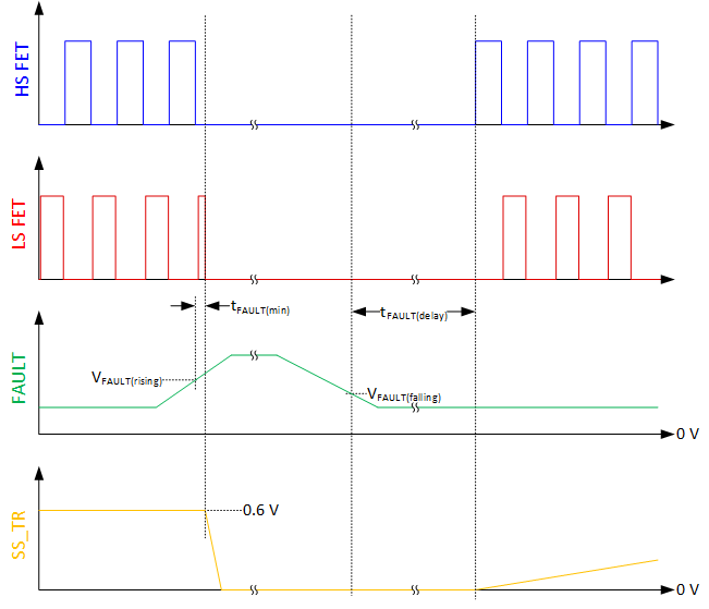
An input FAULT pin is provided to aid in fault management. When the applied voltage exceeds VFAULT(rising) (typically 0.6V) for longer than tFAULT(min) (maximum of 1.4μs), the device stops switching. The device remains in this fault state until the FAULT pin voltage is reduced below VFAULT(falling) (typically 0.5V). Once the fault state is removed, the TPS7H4011 waits tFAULT(delay) seconds (typically 31 switching periods). This delay gives the system time to clear the fault before resuming regulation with soft start.
Figure 8-3 shows an example of the FAULT pin being externally driven high. This can be from a system microcontroller or monitor.
 Figure 8-3 FAULT Pin Waveforms From
External Signal
Figure 8-3 FAULT Pin Waveforms From
External SignalFigure 8-4 shows an example where FAULT is driven by a resistor divider from a monitored voltage (such as VIN or VOUT). By appropriately selecting the resistor divider, FAULT will be triggered when a voltage value is reached. Therefore, the FAULT pin can be configured to provide OVP (overvoltage protection).
 Figure 8-4 FAULT Pin Waveforms From
External Resistor Divider