SLVSAD1B June 2010 – January 2016 TPS80010
PRODUCTION DATA.
- 1 Features
- 2 Applications
- 3 Description
- 4 Revision History
- 5 Pin Configuration and Functions
- 6 Specifications
- 7 Detailed Description
- 8 Application and Implementation
- 9 Power Supply Recommendations
- 10Layout
- 11Device and Documentation Support
- 12Mechanical, Packaging, and Orderable Information
Package Options
Mechanical Data (Package|Pins)
- RSM|32
Thermal pad, mechanical data (Package|Pins)
- RSM|32
Orderable Information
10 Layout
10.1 Layout Guidelines
The VIN_BOOST and VIN_BUCK pins must be bypassed to ground with a low-ESR ceramic bypass capacitor. Texas Instruments recommends the typical bypass capacitance is 10 μF.
- The optimum placement is closest to the VIN_BUCK and VIN_BOOST pins of the device. Minimize the loop area formed by the bypass capacitor connection, the VINDCDC and VINLDO pins, and the thermal pad of the device.
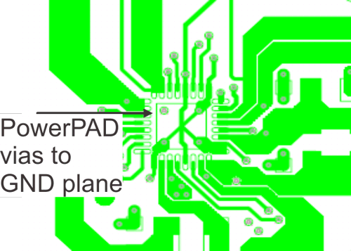
- The thermal pad must be tied to the PCB ground plane with multiple vias.
- The FB _BOOST, FB_BUCK, SW_BOOST, SW_BCUK, and OUT_VM pins (feedback and output pins) traces must be routed away from any potential noise source to avoid coupling.
- Output capacitance must be placed immediately at the output pins. Excessive distance from the capacitance to output pins may cause poor converter performance.
10.2 Layout Example
 Figure 16. TPS80010 Layout