SLVSAI0J October 2010 – May 2016 TPS82670 , TPS82671 , TPS826711 , TPS826716 , TPS82672 , TPS826721 , TPS82673 , TPS82674 , TPS826745 , TPS82675 , TPS82676 , TPS826765 , TPS82677
UNLESS OTHERWISE NOTED, this document contains PRODUCTION DATA.
- 1 Features
- 2 Applications
- 3 Description
- 4 Simplified Schematic
- 5 Revision History
- 6 Device Comparison Table
- 7 Pin Configuration and Functions
- 8 Specifications
- 9 Detailed Description
- 10Applications and Implementation
- 11Power Supply Recommendations
- 12Layout
- 13Device and Documentation Support
- 14Mechanical, Packaging, and Orderable Information
Package Options
Mechanical Data (Package|Pins)
- SIP|8
Thermal pad, mechanical data (Package|Pins)
Orderable Information
12 Layout
12.1 Layout Guidelines
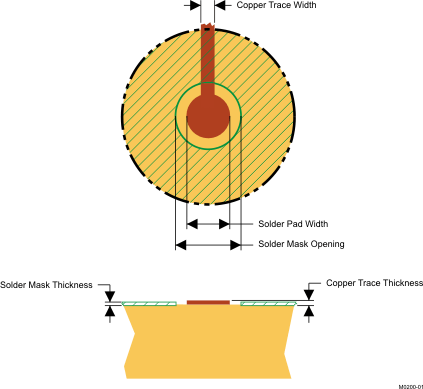
In making the pad size for the µSiP LGA balls, it is recommended that the layout use non-solder-mask defined (NSMD) land. With this method, the solder mask opening is made larger than the desired land area, and the opening size is defined by the copper pad width. Figure 43 shows the appropriate diameters for a MicroSiPTM layout.
12.2 Layout Example
 Figure 43. Recommended Land Pattern Image And Dimensions
| SOLDER PAD DEFINITIONS(1)(2)(3)(4) | COPPER PAD | SOLDER MASK (5)
OPENING |
COPPER THICKNESS | STENCIL (6)
OPENING |
STENCIL THICKNESS |
|---|---|---|---|---|---|
| Non-solder-mask defined (NSMD) | 0.30mm | 0.360mm | 1oz max (0.032mm) | 0.34mm diameter | 0.1mm thick |
12.3 Surface Mount Information
The TPS8267x MicroSiP™ DC/DC converter uses an open frame construction that is designed for a fully automated assembly process and that features a large surface area for pick and place operations. See the "Pick Area" in the package drawings.
Package height and weight have been kept to a minimum thereby to allow the MicroSiP™ device to be handled similarly to a 0805 component.
See JEDEC/IPC standard J-STD-20b for reflow recommendations.