-
TPS8267x 600-mA, High-Efficiency MicroSiP Step-Down Converter (Profile <1.0mm)
- 1 Features
- 2 Applications
- 3 Description
- 4 Simplified Schematic
- 5 Revision History
- 6 Device Comparison Table
- 7 Pin Configuration and Functions
- 8 Specifications
- 9 Detailed Description
- 10Applications and Implementation
- 11Power Supply Recommendations
- 12Layout
- 13Device and Documentation Support
- 14Mechanical, Packaging, and Orderable Information
- IMPORTANT NOTICE
Package Options
Mechanical Data (Package|Pins)
- SIP|8
Thermal pad, mechanical data (Package|Pins)
Orderable Information
TPS8267x 600-mA, High-Efficiency MicroSiP Step-Down Converter (Profile <1.0mm)
1 Features
- 90% Efficiency at 5.5 MHz Operation
- 17μA Quiescent Current
- Wide VIN Range From 2.3 V to 4.8 V
- 5.5MHz Regulated Frequency Operation
- Spread Spectrum, PWM Frequency Dithering
- Best in Class Load and Line Transient
- ±2% Total DC Voltage Accuracy
- Automatic PFM/PWM Mode Switching
- Low Ripple Light-Load PFM Mode
- ≥35dB VIN PSRR (1kHz to 10kHz)
- Internal Soft Start, 120-µs Start-Up Time
- Integrated Active Power-Down Sequencing (Optional)
- Current Overload and Thermal Shutdown Protection
- Sub 1-mm Profile Solution
- Total Solution Size <6.7 mm2
2 Applications
- Cell Phones, Smart-Phones
- Camera Module, Optical Data Module
- Wearable Electronics
- Digital TV, WLAN, GPS and Bluetooth™ Applications
- POL Applications
3 Description
The TPS8267x device is a complete 600mA, DC/DC step-down power supply intended for low-power applications. Included in the package are the switching regulator, inductor and input/output capacitors. No additional components are required to finish the design.
The TPS8267x is based on a high-frequency synchronous step-down dc-dc converter optimized for battery-powered portable applications. The MicroSiP™ DC/DC converter operates at a regulated 5.5-MHz switching frequency and enters the power-save mode operation at light load currents to maintain high efficiency over the entire load current range.
The PFM mode extends the battery life by reducing the quiescent current to 17μA (typ) during light load operation. For noise-sensitive applications, the device has PWM spread spectrum capability providing a lower noise regulated output, as well as low noise at the input. These features, combined with high PSRR and AC load regulation performance, make this device suitable to replace a linear regulator to obtain better power conversion efficiency.
The TPS8267x is packaged in a compact (2.3mm x 2.9mm) and low profile (1.0mm) BGA package suitable for automated assembly by standard surface mount equipment.
Device Information(1)
| PART NUMBER | PACKAGE | BODY SIZE (NOM) |
|---|---|---|
| TPS8267x | µSIP (8) | 2.30 x 2.90 mm |
- For all available packages, see the orderable addendum at the end of the datasheet.
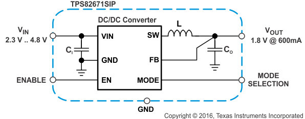
4 Simplified Schematic
|
spacer |
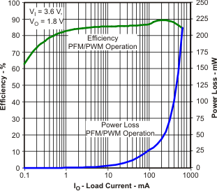
Efficiency vs Output Current |
|
|
spacer |
||
 |
||
5 Revision History
Changes from I Revision (November 2014) to J Revision
- Added TPS8267195 part number to data sheet Go
- Added TPS8267195 to Electrical Characteristics table Go
- Changed Layout Example figure, Note 4 value from "...less than 0.5 mm.." to "...less than 0.5 µm.." Go
Changes from H Revision (October 2014) to I Revision
- Moved Tstg spec to Absolute Maximum Ratings table for clarification Go
- Changed Handling Ratings to ESD Ratings and replaced MIN/MAX values with ± VALUE for clarification Go
- Added TPS826716 data and removed Product Preview note. Go
Changes from G Revision (September 2014) to H Revision
- Added TPS826716 to Device Comparison Table as Product Preview.Go
Changes from F Revision (November 2012) to G Revision
- Added Device Information and Handling Rating tables, Feature Description section, Device Functional Modes, Application and Implementation section, Power Supply Recommendations section, Layout section, Device and Documentation Support section, and Mechanical, Packaging, and Orderable Information section. Go
- Added device TPS826721 Go
Changes from E Revision (October 2012) to F Revision
- Added TPS826745 to HeaderGo
Changes from D Revision (April 2012) to E Revision
- Added TPS826765 to HeaderGo
Changes from C Revision (November 2011) to D Revision
- Added devices TPS82670, TPS82673, and TPS82674 to Header Go
Changes from B Revision (August 2011) to C Revision
- Added device TPS82672 to Header infoGo
Changes from A Revision (April 2011) to B Revision
- Added TPS82676 part number to data sheet header Go
Changes from * Revision (October 2010) to A Revision
6 Device Comparison Table
| PART NUMBER (1) | OUTPUT VOLTAGE | DEVICE SPECIFIC FEATURE | PACKAGE MARKING |
|---|---|---|---|
| TPS82670 | 1.86V | PWM Spread Spectrum Modulation Low PFM Output Ripple Voltage Output Capacitor Discharge |
YK |
| TPS82671 | 1.8V | PWM Spread Spectrum Modulation Low PFM Output Ripple Voltage |
RA |
| TPS826711 | 1.8V | PWM Spread Spectrum Modulation Low PFM Output Ripple Voltage Output Capacitor Discharge |
YW |
| TPS826716 | 1.6V | PWM Spread Spectrum Modulation Low PFM Output Ripple Voltage |
GS |
| TPS82672 | 1.5V | PWM Spread Spectrum Modulation Low PFM Output Ripple Voltage |
WD |
| TPS826721 | 2.1V | PWM Spread Spectrum Modulation Low PFM Output Ripple Voltage |
EO |
| TPS82673 | 1.26V | PWM Spread Spectrum Modulation Low PFM Output Ripple Voltage Output Capacitor Discharge |
YL |
| TPS82674 | 1.2V | PWM Spread Spectrum Modulation Low PFM Output Ripple Voltage Output Capacitor Discharge |
SW |
| TPS826745 | 1.225V | PWM Spread Spectrum Modulation Low PFM Output Ripple Voltage Output Capacitor Discharge |
B5 |
| TPS82675 | 1.2V | PWM Spread Spectrum Modulation Low PFM Output Ripple Voltage |
RB |
| TPS82676 | 1.1V | PWM Spread Spectrum Modulation Low PFM Output Ripple Voltage Output Capacitor Discharge |
TU |
| TPS826765 | 1.05V | PWM Spread Spectrum Modulation Low PFM Output Ripple Voltage Output Capacitor Discharge |
AN |
| TPS82677 | 1.2V | Output Capacitor Discharge | SK |
| TPS8267195 | 1.95V | PWM Spread Spectrum Modulation Low PFM Output Ripple Voltage |
4A |
7 Pin Configuration and Functions
space

space
Pin Functions
| PIN | I/O | DESCRIPTION | |
|---|---|---|---|
| NAME | NO. | ||
| VOUT | A1 | O | Power output pin. Apply output load between this pin and GND. |
| VIN | A2, A3 | I | The VIN pins supply current to the TPS8267x internal regulator. |
| EN | B2 | I | This is the enable pin of the device. Connect this pin to ground to force the converter into shutdown mode. Pull this pin to VI to enable the device. This pin must not be left floating and must be terminated. |
| MODE | B1 | I | This is the mode selection pin of the device. This pin must not be left floating and must be terminated. |
| MODE = LOW: The device is operating in regulated frequency pulse width modulation mode (PWM) at high-load currents and in pulse frequency modulation mode (PFM) at light load currents. | |||
| MODE = HIGH: Low-noise mode is enabled and regulated frequency PWM operation is forced. | |||
| GND | C1, C2, C3 | – | Ground pin. |