SLVSBR0C October   2014  – June 2015 TPS8268090 , TPS8268105 , TPS8268120 , TPS8268150 , TPS8268180

PRODUCTION DATA.  

  1. Features
  2. Applications
  3. Description
  4. Revision History
  5. Device Comparison Table
  6. Pin Configuration and Functions
  7. Specifications
    1. 7.1 Absolute Maximum Ratings
    2. 7.2 ESD Ratings
    3. 7.3 Recommended Operating Conditions
    4. 7.4 Thermal Information
    5. 7.5 Electrical Characteristics
    6. 7.6 Timing Requirements
    7. 7.7 Typical Characteristics
  8. Detailed Description
    1. 8.1 Overview
    2. 8.2 Functional Block Diagram
    3. 8.3 Feature Description
      1. 8.3.1 Soft Start
      2. 8.3.2 Undervoltage Lockout
      3. 8.3.3 Short-Circuit Protection
      4. 8.3.4 Thermal Shutdown
      5. 8.3.5 Enable
      6. 8.3.6 MODE Pin
    4. 8.4 Device Functional Modes
      1. 8.4.1 Spread Spectrum, PWM Frequency Dithering
  9. Application and Implementation
    1. 9.1 Application Information
    2. 9.2 Typical Application
      1. 9.2.1 Design Requirements
      2. 9.2.2 Detailed Design Procedure
        1. 9.2.2.1 Input Capacitor Selection
        2. 9.2.2.2 Output Capacitor Selection
      3. 9.2.3 Application Curves
  10. 10Power Supply Recommendations
  11. 11Layout
    1. 11.1 Layout Guidelines
    2. 11.2 Layout Example
    3. 11.3 Surface Mount Information
    4. 11.4 Thermal and Reliability Information
  12. 12Device and Documentation Support
    1. 12.1 Documentation Support
      1. 12.1.1 References
    2. 12.2 Related Links
    3. 12.3 Trademarks
    4. 12.4 Electrostatic Discharge Caution
    5. 12.5 Glossary
  13. 13Mechanical, Packaging, and Orderable Information
    1. 13.1 Package Summary
    2. 13.2 MicroSiP™ DC/DC Module Package Dimensions

Package Options

Refer to the PDF data sheet for device specific package drawings

Mechanical Data (Package|Pins)
  • SIP|9
Thermal pad, mechanical data (Package|Pins)
Orderable Information

6 Pin Configuration and Functions
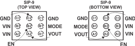
TPS8268180 TPS8268150 TPS8268120 TPS8268105 TPS8268090 po_TPS826x_8x.gif

Pin Functions

PIN I/O DESCRIPTION
NAME NO.
VOUT A1, A2 O Power output pin. Apply output load between this pin and GND.
VIN A3, B3 I Supply voltage connection
EN B2 I This is the enable pin of the device. Connecting this pin low forces the device into shutdown mode. Pulling this pin high enables the device. This pin must not be left floating and must be terminated.
MODE B1 I This pin must be tied to the input supply voltage VIN.
GND C1, C2, C3 Ground pin.