SLVSBR0C October   2014  – June 2015 TPS8268090 , TPS8268105 , TPS8268120 , TPS8268150 , TPS8268180

PRODUCTION DATA.  

  1. Features
  2. Applications
  3. Description
  4. Revision History
  5. Device Comparison Table
  6. Pin Configuration and Functions
  7. Specifications
    1. 7.1 Absolute Maximum Ratings
    2. 7.2 ESD Ratings
    3. 7.3 Recommended Operating Conditions
    4. 7.4 Thermal Information
    5. 7.5 Electrical Characteristics
    6. 7.6 Timing Requirements
    7. 7.7 Typical Characteristics
  8. Detailed Description
    1. 8.1 Overview
    2. 8.2 Functional Block Diagram
    3. 8.3 Feature Description
      1. 8.3.1 Soft Start
      2. 8.3.2 Undervoltage Lockout
      3. 8.3.3 Short-Circuit Protection
      4. 8.3.4 Thermal Shutdown
      5. 8.3.5 Enable
      6. 8.3.6 MODE Pin
    4. 8.4 Device Functional Modes
      1. 8.4.1 Spread Spectrum, PWM Frequency Dithering
  9. Application and Implementation
    1. 9.1 Application Information
    2. 9.2 Typical Application
      1. 9.2.1 Design Requirements
      2. 9.2.2 Detailed Design Procedure
        1. 9.2.2.1 Input Capacitor Selection
        2. 9.2.2.2 Output Capacitor Selection
      3. 9.2.3 Application Curves
  10. 10Power Supply Recommendations
  11. 11Layout
    1. 11.1 Layout Guidelines
    2. 11.2 Layout Example
    3. 11.3 Surface Mount Information
    4. 11.4 Thermal and Reliability Information
  12. 12Device and Documentation Support
    1. 12.1 Documentation Support
      1. 12.1.1 References
    2. 12.2 Related Links
    3. 12.3 Trademarks
    4. 12.4 Electrostatic Discharge Caution
    5. 12.5 Glossary
  13. 13Mechanical, Packaging, and Orderable Information
    1. 13.1 Package Summary
    2. 13.2 MicroSiP™ DC/DC Module Package Dimensions

Package Options

Refer to the PDF data sheet for device specific package drawings

Mechanical Data (Package|Pins)
  • SIP|9
Thermal pad, mechanical data (Package|Pins)
Orderable Information

13 Mechanical, Packaging, and Orderable Information

The following pages include mechanical, packaging, and orderable information. This information is the most current data available for the designated devices. This data is subject to change without notice and revision of this document. For browser-based versions of this data sheet, refer to the left-hand navigation.

13.1 Package Summary

SIP PACKAGE
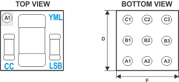
TPS8268180 TPS8268150 TPS8268120 TPS8268105 TPS8268090 PO_top_bott_TPS8268x.gif
Code:
  • CC — Customer Code (device/voltage specific)
  • YML — Y: Year, M: Month, L: Lot trace code
  • LSB — L: Lot trace code, S: Site code, B: Board locator

13.2 MicroSiP™ DC/DC Module Package Dimensions

TheTPS8268x is available in an 9-bump ball grid array (BGA) package. The package dimensions are:

  • D = 2.30 ±0.05 mm
  • E = 2.90 ±0.05 mm