-
TPS8269x High-Efficiency MicroSIP Step-Down Converter (Profile <1 mm)
- 1 Features
- 2 Applications
- 3 Description
- 4 Revision History
- 5 Device Comparison
- 6 Pin Configuration and Functions
- 7 Specifications
- 8 Parameter Measurement Information
- 9 Detailed Description
- 10Application and Implementation
- 11Power Supply Recommendations
- 12Layout
- 13Device and Documentation Support
- 14Mechanical, Packaging, and Orderable Information
- IMPORTANT NOTICE
Package Options
Mechanical Data (Package|Pins)
- SIP|8
Thermal pad, mechanical data (Package|Pins)
Orderable Information
TPS8269x High-Efficiency MicroSIP Step-Down Converter (Profile <1 mm)
1 Features
- Total Solution Size < 6.7 mm2
- 95% Efficiency at 3-MHz Operation
- 23μA Quiescent Current
- High Duty-Cycle Operation
- Best in Class Load and Line Transient
- ±2% Total DC Voltage Accuracy
- Automatic PFM/PWM Mode Switching
- Low Ripple Light-Load PFM Mode
- Excellent AC Load Regulation
- Internal Soft Start, 200-µs Start-Up Time
- Integrated Active Power-Down Sequencing (Optional)
- Current Overload and Thermal Shutdown Protection
- Sub 1-mm Profile Solution
2 Applications
- Cell Phones, Smart-Phones
- Optical Data Modules
- Camera and Sensor Modules
- Wearable Devices
- LDO Replacement
3 Description
The TPS8269xSIP device is a complete 500 mA / 800 mA, DC/DC step-down power supply intended for low-power applications. Included in the package are the switching regulator, inductor and input/output capacitors. No additional components are required to finish the design. The TPS8269xSIP is based on a high-frequency synchronous step-down dc-dc converter optimized for battery-powered portable applications. The MicroSIP™ DC/DC converter operates at a regulated 3-MHz switching frequency and enters the power-save mode operation at light load currents to maintain high efficiency over the entire load current range. The PFM mode extends the battery life by reducing the quiescent current to 23 μA (typical) during light load operation. For noise-sensitive applications, the device has PWM spread spectrum capability providing a lower noise regulated output, as well as low noise at the input. These features, combined with high PSRR and AC load regulation performance, make this device suitable to replace a linear regulator to obtain better power conversion efficiency. The TPS8269xSIP is packaged in a compact (2.9 mm × 2.3 mm) and low profile (1 mm) BGA package suitable for automated assembly by standard surface mount equipment.
Device Information
| ORDER NUMBER | PACKAGE | BODY SIZE |
|---|---|---|
| TPS82692SIP | µSIP (8) | 2,9mm × 2,3mm |
| TPS82693SIP | µSIP (8) | 2,9mm × 2,3mm |
| TPS826951SIP | µSIP (8) | 2,9mm × 2,3mm |
| TPS82697SIP | µSIP (8) | 2,9mm × 2,3mm |
| TPS82698SIP | µSIP (8) | 2,9mm × 2,3mm |
.
Device Images
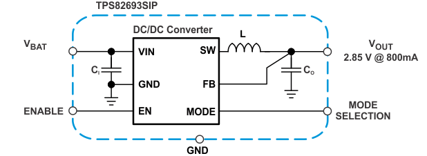
Simplified Schematic

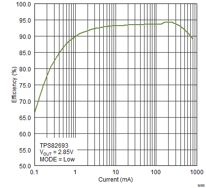
Efficiency vs Output Current

4 Revision History
Changes from B Revision (March 2014) to C Revision
- Added text to Device Comparison table for the TPS826951 device special features Go
- Moved Tstg spec from Handling Ratings to Absolute Maximum Ratings tableGo
- Changed Handling Ratings table to ESD Ratings table Go
Changes from A Revision (July 2013) to B Revision
- Global format to new data sheet standard Go
- Changed TPS82692, TPS826951 devices to production status. Go
- Changed Ordering Information table to "Device Comparison" table with cross reference to the POA at end of document. Go
- Moved Abs Max Ratings, Handling Ratings, Rec Oper Conditions, Thermal Info, and Elec Charactistics tables to the Specifications section Go
- Deleted Regulated DC Output Voltage parameters to electrical characteristics table for device TPS82692Go
- Added efficiency graphs for device TPS82692 Go
Changes from * Revision (March 2013) to A Revision
- Added Regulated DC Output Voltage parameters to electrical characteristics table for device TPS82697Go
- Added Regulated DC Output Voltage parameters to electrical characteristics table for device TPS826951Go
- Added Regulated DC Output Voltage parameters to electrical characteristics table for device TPS82698Go
- Added Power-save mode ripple voltage to electrical characteristics table for devices TPS826951, TPS82697, TPS82698Go
- Added Start-up time to electrical characteristics table for devices TPS826951, TPS82697, TPS82698Go
- Added Efficiency vs Load Current Graph figure references to Table of Graphs. Go
- Added Transient Response Plots to Typical Characteristics for device TPS826951Go
- Added AC Load Transient Response Plots to Typical Characteristics for devices TPS826951, TPS82698Go
5 Device Comparison
6 Pin Configuration and Functions

Pin Functions
| TERMINAL | I/O | DESCRIPTION | |
|---|---|---|---|
| NAME | NO. | ||
| VOUT | A1 | O | Power output terminal. Apply output load between this terminal and GND. |
| VIN | A2, A3 | I | The VIN terminals supply current to the TPS8269xSIP's internal regulator. |
| EN | B2 | I | This is the enable terminal of the device. Connecting this terminal to ground forces the converter into shutdown mode. Pulling this terminal to VIN enables the device. This terminal must not be left floating and must be terminated. |
| MODE | B1 | I | This is the mode selection terminal of the device. This terminal must not be left floating and must be terminated. |
| MODE = LOW: The device is operating in regulated frequency pulse width modulation mode (PWM) at high-load currents and in pulse frequency modulation mode (PFM) at light load currents. | |||
| MODE = HIGH: Low-noise mode enabled, regulated frequency PWM operation forced. | |||
| GND | C1, C2, C3 | – | Ground terminal. |