SLVSF29C October 2019 – August 2021 TPS8804
PRODUCTION DATA
- 1 Features
- 2 Applications
- 3 Description
- 4 Revision History
- 5 Pin Configuration and Functions
- 6 Specifications
-
7 Detailed Description
- 7.1 Overview
- 7.2 Functional Block Diagram
- 7.3 Feature Description
- 7.4 Device Functional Modes
- 7.5 Programming
- 7.6
Register Maps
- 7.6.1 REVID Register (Offset = 0h) [reset = 0h]
- 7.6.2 STATUS1 Register (Offset = 1h) [reset = 0h]
- 7.6.3 STATUS2 Register (Offset = 2h) [reset = 0h]
- 7.6.4 MASK Register (Offset = 3h) [reset = 0h]
- 7.6.5 CONFIG1 Register (Offset = 4h) [reset = 20h]
- 7.6.6 CONFIG2 Register (Offset = 5h) [reset = 0h]
- 7.6.7 ENABLE1 Register (Offset = 6h) [reset = 0h]
- 7.6.8 ENABLE2 Register (Offset = 7h) [reset = 0h]
- 7.6.9 CONTROL Register (Offset = 8h) [reset = 0h]
- 7.6.10 GPIO_AMUX Register (Offset = Bh) [reset = 0h]
- 7.6.11 COSW Register (Offset = Ch) [reset = 0h]
- 7.6.12 CO Register (Offset = Dh) [reset = 0h]
- 7.6.13 LEDLDO Register (Offset = Fh) [reset = 0h]
- 7.6.14 PH_CTRL Register (Offset = 10h) [reset = 0h]
- 7.6.15 LED_DAC_A Register (Offset = 11h) [reset = 0h]
- 7.6.16 LED_DAC_B Register (Offset = 12h) [reset = 0h]
- 8 Application and Implementation
- 9 Power Supply Recommendations
- 10Layout
- 11Device and Documentation Support
- 12Mechanical, Packaging, and Orderable Information
Package Options
Mechanical Data (Package|Pins)
- DCP|38
Thermal pad, mechanical data (Package|Pins)
- DCP|38
Orderable Information
7.3.1 System Power-up
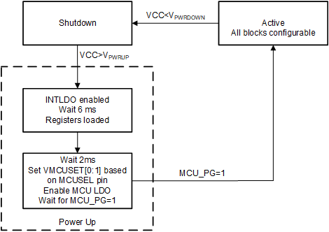
 Figure 7-1 Power-up State Diagram
The TPS8804 can power-up from a DC power supply above 3.6 V connected to the VCC pin. When the VCC voltage exceeds the VPWRUP threshold, the TPS8804 initializes for 6 ms. After the initialization, the MCUSEL pin is sensed for 2 ms to determine the MCULDO voltage and program the VMCUSET register. Table 7-1 indicates the VMCU setting for each MCUSEL configuration. The MCULDO is enabled and the system waits for VMCU to reach its power-good threshold (typically 85% of its target voltage). It is only after VMCU reaches its power-good threshold that I2C communication is allowed with the TPS8804. This sequence of events is outlined in Figure 7-1.
Table 7-1 VMCU Power-up Voltage
| MCUSEL Connection | VMCU (V) |
|---|---|
| 620-Ω to GND | 1.5 |
| Short to GND | 1.8 |
| Short to VINT | 2.5 |
| 330-pF to GND | 3.3 |