SLVSF29C October   2019  – August 2021 TPS8804

PRODUCTION DATA  

  1. Features
  2. Applications
  3. Description
  4. Revision History
  5. Pin Configuration and Functions
    1.     Pin Functions
  6. Specifications
    1. 6.1 Absolute Maximum Ratings
    2. 6.2 ESD Ratings
    3. 6.3 Recommended Operating Conditions
    4. 6.4 Thermal Information
    5. 6.5 Electrical Characteristics
    6. 6.6 Typical Characteristics
  7. Detailed Description
    1. 7.1 Overview
    2. 7.2 Functional Block Diagram
    3. 7.3 Feature Description
      1. 7.3.1 System Power-up
      2. 7.3.2 LDO Regulators
        1. 7.3.2.1 Power LDO Regulator
        2. 7.3.2.2 Internal LDO Regulator
        3. 7.3.2.3 Microcontroller LDO Regulator
      3. 7.3.3 Photo Chamber AFE
        1. 7.3.3.1 Photo Input Amplifier
        2. 7.3.3.2 Photo Gain Amplifier
      4. 7.3.4 LED Driver
        1. 7.3.4.1 LED Current Sink
        2. 7.3.4.2 LED Voltage Supply
      5. 7.3.5 Carbon Monoxide Sensor AFE
        1. 7.3.5.1 CO Transimpedance Amplifier
        2. 7.3.5.2 CO Connectivity Test
      6. 7.3.6 SLC Interface Transmitter and Receiver
        1. 7.3.6.1 SLC Transmitter
        2. 7.3.6.2 SLC Receiver
      7. 7.3.7 AMUX
      8. 7.3.8 Analog Bias Block and 8 MHz Oscillator
      9. 7.3.9 Interrupt Signal Alerts
    4. 7.4 Device Functional Modes
      1. 7.4.1 Fault States
        1. 7.4.1.1 MCU LDO Fault
        2. 7.4.1.2 Over-Temperature Fault
    5. 7.5 Programming
    6. 7.6 Register Maps
      1. 7.6.1  REVID Register (Offset = 0h) [reset = 0h]
      2. 7.6.2  STATUS1 Register (Offset = 1h) [reset = 0h]
      3. 7.6.3  STATUS2 Register (Offset = 2h) [reset = 0h]
      4. 7.6.4  MASK Register (Offset = 3h) [reset = 0h]
      5. 7.6.5  CONFIG1 Register (Offset = 4h) [reset = 20h]
      6. 7.6.6  CONFIG2 Register (Offset = 5h) [reset = 0h]
      7. 7.6.7  ENABLE1 Register (Offset = 6h) [reset = 0h]
      8. 7.6.8  ENABLE2 Register (Offset = 7h) [reset = 0h]
      9. 7.6.9  CONTROL Register (Offset = 8h) [reset = 0h]
      10. 7.6.10 GPIO_AMUX Register (Offset = Bh) [reset = 0h]
      11. 7.6.11 COSW Register (Offset = Ch) [reset = 0h]
      12. 7.6.12 CO Register (Offset = Dh) [reset = 0h]
      13. 7.6.13 LEDLDO Register (Offset = Fh) [reset = 0h]
      14. 7.6.14 PH_CTRL Register (Offset = 10h) [reset = 0h]
      15. 7.6.15 LED_DAC_A Register (Offset = 11h) [reset = 0h]
      16. 7.6.16 LED_DAC_B Register (Offset = 12h) [reset = 0h]
  8. Application and Implementation
    1. 8.1 Application Information
    2. 8.2 Typical Application
      1. 8.2.1 Design Requirements
      2. 8.2.2 Detailed Design Procedure
        1. 8.2.2.1 Photo Amplifier Component Selection
        2. 8.2.2.2 LED Driver Component Selection
        3. 8.2.2.3 LED Voltage Supply Selection
        4. 8.2.2.4 Regulator Component Selection
      3. 8.2.3 Application Curves
  9. Power Supply Recommendations
  10. 10Layout
    1. 10.1 Layout Guidelines
      1. 10.1.1 Photo Amplifier Layout
      2. 10.1.2 CO Amplifier Layout
      3. 10.1.3 Ground Plane Layout
    2. 10.2 Layout Example
  11. 11Device and Documentation Support
    1. 11.1 Receiving Notification of Documentation Updates
    2. 11.2 Support Resources
    3. 11.3 Trademarks
    4. 11.4 Electrostatic Discharge Caution
    5. 11.5 Glossary
  12. 12Mechanical, Packaging, and Orderable Information

Package Options

Mechanical Data (Package|Pins)
Thermal pad, mechanical data (Package|Pins)
Orderable Information

SLC Interface Transmitter and Receiver

GUID-59DEA7BF-66D3-4B92-9FD0-8CED0D75B134-low.gif
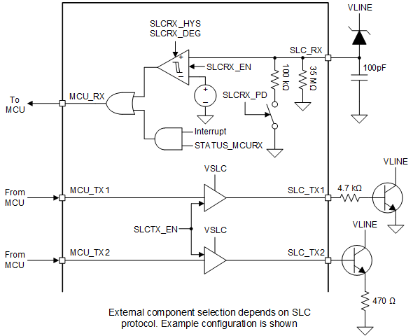
External component selection depends on SLC protocol. Example configuration is shown
Figure 7-6 SLC Interface Circuit

In smoke detection systems where the power line carries communication signals between smoke detectors and central fire panels, the SLC interface connects to the power line to transmit and receive data from the MCU. The interface isolates the high voltage power line from the microcontroller, mitigating risk of damage and reducing external component count.