TPS92411x Floating Switch for Offline AC Linear Direct Drive of LEDs with Low Ripple Current
1 Features
- High-Performance Solution for Driving LEDs from AC Mains
- Simplifies Design of Phase Dimmable LED Driver with High Power Factor, Low Total Harmonic Distortion, and Low Current Ripple
- Suitable for LED Luminaires up to 70+ W
- Input Voltage Range: 7.5 V to 100 V
- Stackable 100 V, 2-Ω MOSFET Building Block
- Controlled Switch Open and Close Transitions Minimize EMI
- Designed for use with the TPS92410 or with a Discrete Linear Regulator
- Input Undervoltage Protection
- Output Overvoltage Protection (TPS92411P)
- Low IQ: 200 µA (typ)
2 Applications
- LED Lamps and Light Bulbs
- LED Luminaires
- Downlights
3 Description
The TPS92411 is a 100-V floating MOSFET switch for use in offline LED lighting applications. The device is used in conjunction with a current regulator that can achieve a power factor greater than 0.9 to create a LED drive solution with low-ripple current. When properly designed, solution performance is comparable to traditional flyback, buck or boost-based AC/DC LED drivers. The approach requires no inductive components, thus saving size and cost. Slew-controlled low-frequency operation of the TPS92411 switches creates very little EMI. Detailed operation is described in the Application Information section.
Package options include SOT23-5 and PSOP-8 allowing the user to optimize for small size or scale for high power. Using the PSOP-8 package, design of LED luminaires up to 70 W or more is possible. Other features include a UVLO circuit to monitor when the device has sufficient voltage to operate properly and over-voltage protection (TPS92411P).
Device Information(1)
| PART NUMBER | PACKAGE | BODY SIZE (NOM) |
|---|---|---|
| TPS92411, TPS92411P | SOT-23 (5) | 2.90 mm x 1.60 mm |
| SO PowerPAD (8) | 4.89 mm x 3.90 mm |
- For all available packages, see the orderable addendum at the end of the datasheet.

4 Revision History
Changes from A Revision (May 2014) to B Revision
- Added Pin Configuration and Functions section, Handling Rating table, Feature Description section, Device Functional Modes, Application and Implementation section, Power Supply Recommendations section, Layout section, Device and Documentation Support section, and Mechanical, Packaging, and Orderable Information section Go
Changes from * Revision (October 2013) to A Revision
5 Pin Configuration and Functions
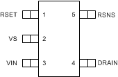
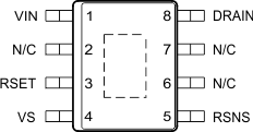
Pin Functions
| PIN | I/O | DESCRIPTION | ||
|---|---|---|---|---|
| NAME | NO. | |||
| DDA | DBV | |||
| DRAIN | 8 | 4 | O | Drain of the internal switch. |
| N/C | 2 | — | — | Not internally connected. |
| N/C | 6 | |||
| N/C | 7 | |||
| VIN | 1 | 3 | I | Positive power supply for the device. |
| VS | 4 | 2 | I/O | Source of the internal switch. This pin is also the device floating ground. |
| RSET | 3 | 1 | I/O | A resistor connected between the RSET pin and the VIN pin sets the rising threshold to open the switch. |
| RSNS | 5 | 5 | I/O | A resistor connected between the RSNS pin to system ground senses the VS voltage relative to system ground. |
| Exposed Themal Pad | Connect to VS pin directly beneath the device. | |||
6 Specifications
6.1 Absolute Maximum Ratings
All voltages are with respect to VS, –40 °C < TJ = TA ≤ 150 °C. All currents are positive into and negative out of the specified terminal (unless otherwise noted).| MIN | MAX | UNIT | ||
|---|---|---|---|---|
| Supply voltage | VIN | –0.3 | 105 | V |
| Switch voltage | DRAIN | –0.3 | 105 | |
| Junction temperature | TJ | –40 | 165 | ºC |
6.2 Handling Ratings
| MIN | MAX | UNIT | |||
|---|---|---|---|---|---|
| Tstg | Storage temperature range | –65 | 150 | °C | |
| V(ESD) | Electrostatic discharge | Human body model (HBM), per ANSI/ESDA/JEDEC JS-001, all pins(1) | 1 | kV | |
| Charged device model (CDM), per JEDEC specification JESD22-C101, all pins(2) | 250 | V | |||
6.3 Recommended Operating Conditions
Over operating free-air temperature range (unless otherwise noted)| MIN | TYP | MAX | UNIT | |||
|---|---|---|---|---|---|---|
| VIN | Input voltage | TPS92411P | 7.5 | 94 | V | |
| TPS92411 | 7.5 | 100 | ||||
| TJ | Operating junction temperature | –40 | 25 | 150 | °C | |
6.4 Thermal Information
| THERMAL METRIC(1) | TPS92411 | UNIT | ||
|---|---|---|---|---|
| DBV | DDA | |||
| 5 PINS | 8 PINS | |||
| θJA | Junction-to-ambient thermal resistance(2) | 209.8 | 58.6 | °C/W |
| θJCtop | Junction-to-case (top) thermal resistance(3) | 125.2 | 72 | |
| θJB | Junction-to-board thermal resistance(4) | 38 | 39.1 | |
| ψJT | Junction-to-top characterization parameter(5) | 15.6 | 21.6 | |
| ψJB | Junction-to-board characterization parameter(6) | 37.1 | 39.1 | |
| θJCbot | Junction-to-case (bottom) thermal resistance(7) | N/A | 15 | |
6.5 Electrical Characteristics
Unless otherwise specified –40 °C ≤ TJ = TA ≤ 150 °C, (VVIN – VVS) = 30 V, RRSET = RRSNS = Open, all voltages are with respect to VS.| PARAMETER | TEST CONDITIONS | MIN | TYP | MAX | UNIT | ||
|---|---|---|---|---|---|---|---|
| INPUT SUPPLY (VIN) | |||||||
| VIN(ovp) | Input overvoltage protection | TPS92411P | Rising threshold | 95 | 100 | V | |
| Falling threshold | 96 | ||||||
| Hysteresis | 4 | ||||||
| IQ | Bias current | 200 | 400 | μA | |||
| VIN(uvlo) | Input undervoltage lockout | Rising threshold | 6.5 | 7 | V | ||
| VIN(hys) | Input UVLO hysteresis | 370 | mV | ||||
| SWITCH CONTROL (RSNS, RSET) | |||||||
| IRSNS | RSNS threshold current | –3.3 | –4 | –4.9 | μA | ||
| VRSNS_OS | RSNS offset voltage | 165 | 210 | 255 | mV | ||
| VRSET | RSET threshold voltage | 1.2 | 1.25 | 1.3 | V | ||
| IRSET | RSET current | IRSNS = –20 μA, (VRSET – VVS) = 1.5 V | –9.3 | –10 | –10.7 | μA | |
| IRSNS = –40 μA, (VRSET – VVS) = 1.5 V | –19 | –20 | –21 | ||||
| IRSNS = –100 μA, (VRSET – VVS) = 1.5 V | –47.9 | –50 | –52.1 | ||||
| SWITCH (DRAIN, VS) | |||||||
| RDS(on) | On-resistance | IDRAIN = 100 mA, TJ = 25°C | 1 | 2 | 2.5 | Ω | |
| dv/dt(ON) | Switch ON slew rate | (VDRAIN – VVS) falling 36 V to 4 V, ISW = 100 mA |
1 | V/μs | |||
| dv/dt(OFF) | Switch OFF slew rate | (VDRAIN – VVS) = rising 4 V to 36 V, ISW = 100 mA |
0.5 | ||||
6.6 Typical Characteristics
Unless otherwise stated, –40 °C ≤ TA = TJ ≤ 150 °C, (VVIN – VVS) = 30 V, all voltages are with respect to VS. Figure 1. UVLO vs. Temperature
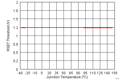 Figure 3. RSET Threshold vs. Temperature
 Figure 5. Switch On-Resistance (RDS(on)) vs. Temperature
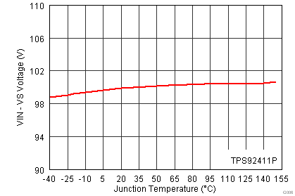 Figure 7. (VVIN – VVS) Overvoltage Threshold vs. Temperature
 Figure 2. UVLO vs. Temperature
 Figure 4. RSNS Threshold Current vs. Temperature
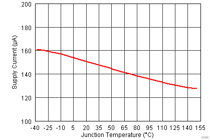 Figure 6. Input Voltage Quiescent Current vs. Temperature
7 Detailed Description
7.1 Overview
The TPS92411 is an advanced, floating driver specifically designed for use with a linear regulator in low-power offline LED lighting applications. It integrates an on-board 100-V MOSFET switch to shunt LED current as the line transitions. As the line transitions through the cycle, the device monitors critical nodes for zero cross at which time the internal switch is either opened or shorted to steer the current through or away from the LED stack. The TPS92411 does not directly control output power or LED current, it just directs current to the LED stack or bypasses the LED stack.
7.2 Functional Block Diagram
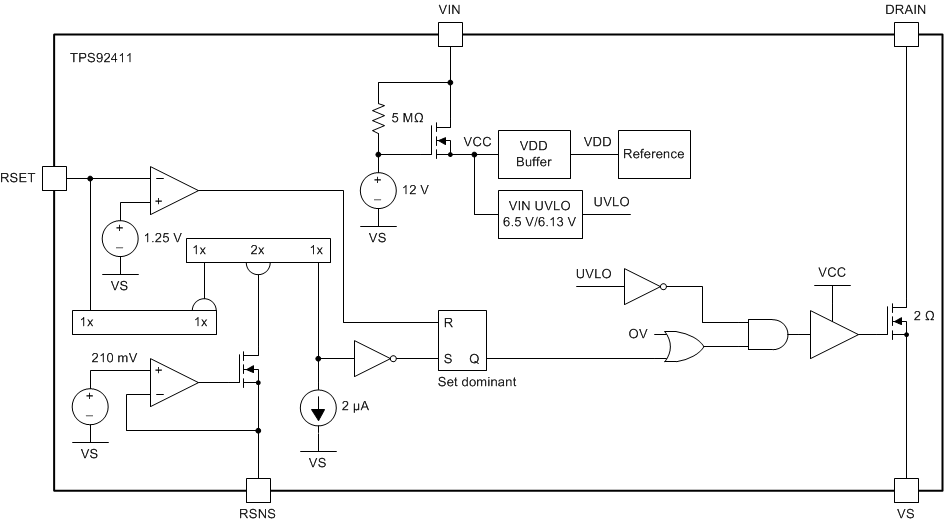 Figure 8. TPS92411 Block Diagram
 Figure 9. TPS92411P Block Diagram
7.3 Feature Description
7.3.1 Overvoltage Protection (OVP)
Overvoltage protection (OVP) in the TPS92411P version protects the device as well as the LEDs and storage capacitor. The OVP is set at approximately 100 V (VVIN – VVS) and closes the internal switch when the threshold voltage is reached. For this reason LED stack voltages of 94 V or less are recommended. Higher voltages can be used with the TPS92411 version but tolerances must be considered to ensure that the 105 V absolute maximum rating is not exceeded.
7.3.2 Input Undervoltage Lockout (UVLO)
The TPS92411 includes input UVLO. The UVLO prevents the device from operation until the VIN pin voltage with respect to VS exceeds 6.5 V and ensures the device behaves properly when enabled.
7.3.3 LED Capacitor
A capacitor is required across each LED stack to provide current to the LEDs during the switch ON time. Refer to the available calculator software (SLVC516 for 120-V applications or SLVC517 for 230-V applications) for calculating the minimum value required for any particular application. The software calculates the minimum value required for a particular application, but best performance is acheived by using as much capacitance as possible given size and cost constraints. These design tools also calculate a minimum value for any given current ripple percent or flicker index desired for the particular application.
7.3.4 Blocking Diode
A blocking diode is required between the drain of the switch (DRAIN) and the anode of the LED stack. This prevents the LED capacitor from discharging through the switch during the switch ON time instead allowing it to discharge through the LED stack. This diode should be rated for 200 V reverse voltage and capable of forward currents as high as the average linear regulator current setting.
7.4 Device Functional Modes
The TPS92411P has 4 functional modes while the TPS92411 has 3:
7.4.1 Input UVLO
As described in the previous section the device and internal switch will remain off until VIN is 6.5V or greater with respect to VS.
7.4.2 Operating with Internal Switch ON
After the device crosses the UVLO threshold the internal switch will turn on and remain on until the voltage at the VIN pin exceeds the threshold voltage set by the RSET resistor.
7.4.3 Operating with Internal Switch OFF
When the RSET threshold voltage is exceeded on the VIN pin the internal switch will turn off forcing all the current to flow through the LEDs and charge the LED capacitor. The switch will remain off until the VS pin drops below the threshold voltage set by RSNS or an overvoltage event occurs (TPS92411P only).
7.4.4 Overvoltage Operation (TPS92411P)
If an LED fails open or a string voltage exceeding the OVP level is used the device will enter OVP operation. The internal switch will close and remain closed until the VIN voltage with respect to the VS pin drops low enough to engage normal operation again.
