SLUSBZ6A April   2016  – August 2016 TPS92515 , TPS92515-Q1 , TPS92515HV , TPS92515HV-Q1

PRODUCTION DATA.  

  1. Features
  2. Applications
  3. Description
    1.     Simplified Buck LED Driver Application
  4. Revision History
  5. Device Comparison Table
  6. Pin Configuration and Functions
    1. Table 1. Pin Functions
  7. Specifications
    1. 7.1 Absolute Maximum Ratings
    2. 7.2 ESD Ratings
    3. 7.3 Recommended Operating Conditions
    4. 7.4 Thermal Information
    5. 7.5 Electrical Characteristics
    6. 7.6 Typical Characteristics
  8. Detailed Description
    1. 8.1 Overview
    2. 8.2 Functional Block Diagram
    3. 8.3 Feature Description
      1. 8.3.1  General Operation
      2. 8.3.2  Current Sense Comparator
      3. 8.3.3  OFF Timer
      4. 8.3.4  OFF-Timer, Shunt FET Dimming or Shunted Output Condition
      5. 8.3.5  Internal N-channel MOSFET
        1. 8.3.5.1 Drop-Out
      6. 8.3.6  VCC Internal Regulator and Undervoltage Lockout (UVLO)
      7. 8.3.7  Analog Adjust Input
        1. 8.3.7.1 IADJ Pin Clamp
        2. 8.3.7.2 IADJ Pin Clamp Characteristic
        3. 8.3.7.3 Analog Adjust (IADJ Pin) Control Methods
        4. 8.3.7.4 IADJ Control Method Notes
      8. 8.3.8  Thermal Protection
        1. 8.3.8.1 Maximum Output Current and Junction Temperature
      9. 8.3.9  Junction Temperature Relative Estimation
      10. 8.3.10 BOOT and BOOT UVLO
        1. 8.3.10.1 Start-Up, BOOT-UVLO and Pre-Charged Condition
      11. 8.3.11 PWM (UVLO and Enable)
        1. 8.3.11.1 Using PWM for UVLO (Undervoltage Lockout) Protection
          1. 8.3.11.1.1 UVLO Programming Resistors
        2. 8.3.11.2 Using PWM for Digitally Controlled Enable
        3. 8.3.11.3 UVLO: VIN, VCC and BOOT UVLO
        4. 8.3.11.4 Analog and PWM Dimming - Normalized Results and Comparison
    4. 8.4 Device Functional Modes
  9. Application and Implementation
    1. 9.1 Application Information
    2. 9.2 Typical Application
      1. 9.2.1 General Design Procedure
        1. 9.2.1.1 Calculating Duty Cycle
        2. 9.2.1.2 Calculate OFF-Time Estimate
        3. 9.2.1.3 Calculate OFF-Time Resistor ROFF
        4. 9.2.1.4 Calculate the Minimum Inductance Value
        5. 9.2.1.5 Calculate the Sense Resistance
        6. 9.2.1.6 Calculate Input Capacitance
        7. 9.2.1.7 Calculate Output Capacitance
      2. 9.2.2 Design Requirements
      3. 9.2.3 Detailed Design Procedure
        1. 9.2.3.1 Calculating Duty Cycle
        2. 9.2.3.2 Calculate OFF-Time Estimate
        3. 9.2.3.3 Calculate OFF-Time Resistor ROFF
        4. 9.2.3.4 Calculate the Inductance Value
        5. 9.2.3.5 Calculate the Sense Resistance
        6. 9.2.3.6 Calculate Input Capacitance
        7. 9.2.3.7 Verify Peak Current for Inductor Selection
        8. 9.2.3.8 Calculate Output Capacitance
        9. 9.2.3.9 Calculate UVLO Resistance Values
      4. 9.2.4 Application Curves
    3. 9.3 Dos and Don'ts
  10. 10Power Supply Recommendations
    1. 10.1 Input Source Direct from Battery
    2. 10.2 Input Source from a Boost Stage
  11. 11Layout
    1. 11.1 Layout Guidelines
    2. 11.2 Layout Example
  12. 12Device and Documentation Support
    1. 12.1 Documentation Support
      1. 12.1.1 Related Documentation
        1. 12.1.1.1 Related Links
    2. 12.2 Receiving Notification of Documentation Updates
    3. 12.3 Community Resources
    4. 12.4 Trademarks
    5. 12.5 Electrostatic Discharge Caution
    6. 12.6 Glossary
  13. 13Mechanical, Packaging, and Orderable Information

Package Options

Mechanical Data (Package|Pins)
Thermal pad, mechanical data (Package|Pins)
Orderable Information

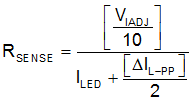
Calculate the Sense Resistance

Always use the highest VIADJ voltage the application allows without exceeding 5.5 V. The device clamps any higher value to a level 2.4 V. See also the Analog Adjust Input for details.

Equation 20. TPS92515 TPS92515-Q1 TPS92515HV TPS92515HV-Q1 Rsense.gif