SLUSEG1A August 2021 – December 2021 TPS92519-Q1
PRODUCTION DATA
- 1 Features
- 2 Applications
- 3 Description
- 4 Revision History
- 5 Pin Configuration and Functions
- 6 Specifications
-
7 Detailed Description
- 7.1 Overview
- 7.2 Functional Block Diagram
- 7.3
Feature Description
- 7.3.1 Buck Converter Switching Operation
- 7.3.2 Switching Frequency and Adaptive On-Time Control
- 7.3.3 Minimum On-Time, Off-Time, and Inductor Ripple
- 7.3.4 Enable
- 7.3.5 LED Current Regulation and Error Amplifier
- 7.3.6 Start-up Sequence
- 7.3.7 Analog Dimming and Forced Continuous Conduction Mode
- 7.3.8 External PWM Dimming and Input Undervoltage Lockout (UVLO)
- 7.3.9 Shunt FET Dimming or Matrix Beam Application
- 7.3.10 Bias Supply
- 7.3.11 Bootstrap Supply
- 7.3.12 Faults and Diagnostics
- 7.3.13 Output Short Circuit Fault
- 7.3.14 Output Open Circuit Fault
- 7.3.15 Parallel Operation
- 7.4 Device Functional Modes
-
8 Application and Implementation
- 8.1
Application Information
- 8.1.1 Duty Cycle Consideration
- 8.1.2 Switching Frequency Selection
- 8.1.3 LED Current Set Point
- 8.1.4 Inductor Selection
- 8.1.5 Output Capacitor Selection
- 8.1.6 Input Capacitor Selection
- 8.1.7 Bootstrap Capacitor Selection
- 8.1.8 Compensation Capacitor Selection
- 8.1.9 Input Undervoltage Protection
- 8.1.10 CSN Protection Diode
- 8.2
Typical Application
- 8.2.1 Design Requirements
- 8.2.2
Detailed Design Procedure
- 8.2.2.1 Calculating Duty Cycle
- 8.2.2.2 Calculating Minimum On-Time and Off-Time
- 8.2.2.3 Minimum Switching Frequency
- 8.2.2.4 LED Current Set Point
- 8.2.2.5 Inductor Selection
- 8.2.2.6 Output Capacitor Selection
- 8.2.2.7 Bootstrap Capacitor Selection
- 8.2.2.8 Compensation Capacitor Selection
- 8.2.2.9 PWM Dimming and Input Voltage Protection
- 8.2.3 Application Curves
- 8.1
Application Information
- 9 Power Supply Recommendations
- 10Layout
- 11Device and Documentation Support
- 12Mechanical, Packaging, and Orderable Information
Package Options
Mechanical Data (Package|Pins)
- DAP|32
Thermal pad, mechanical data (Package|Pins)
- DAP|32
Orderable Information
3 Description
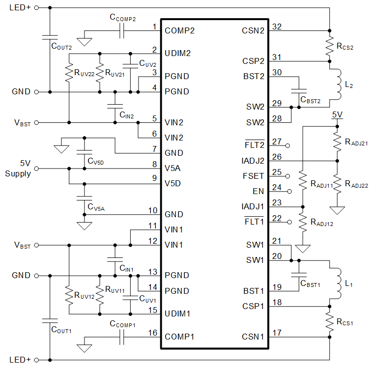
The TPS92519-Q1 is a monolithic dual synchronous
buck LED driver with a wide 4.5-V to 65-V operating input voltage range that can
independently power two strings of series connected LEDs. The
TPS92519-Q1 implements an adaptive on-time average current mode control and is designed to
be compatible with shunt FET dimming techniques and LED matrix manager-based dynamic beam
headlamps. The adaptive on-time control provides near constant switching frequency that can
be set using FSET input. Inductor current sensing and closed-loop feedback enables better
than ±4% accuracy over wide input voltage, output voltage and ambient temperature range.
The high performance LED driver can independently modulate LED current using both analog or PWM dimming techniques. Linear analog dimming response with over 16:1 range is obtained by varying the voltage from 140 mV to 2.45 V across the high Impedance Analog Adjust (IADJ) input. PWM dimming of LED current is achieved by directly modulating the corresponding UDIM input pin with the desired duty cycle and frequency. The device supports high frequency shunt FET dimming and is compatible with pixel control techniques using LED matrix manager.
The TPS92519-Q1 supports parallel operation of two or more channels thus enabling flexibility required to drive high current LEDs or laser diodes. Current is shared between parallel channels based on IADJ input independent of component tolerances and parasitics.
The TPS92519-Q1 incorporates advanced fault protection featuring: cycle-by-cycle switch current limit, bootstrap undervoltage and thermal shutdown. The device includes an open drain fault output to indicate output open and short conditions.
The TPS92519-Q1 is available in a 8.1-mm × 11-mm thermally-enhanced 32-pin HTSSOP package with a 2.75-mm × 3.45-mm bottom-exposed pad.
| PART NUMBER(1) | PACKAGE | BODY SIZE (NOM) |
|---|---|---|
| TPS92519-Q1 | HTSSOP | 8.1 mm × 11 mm |
 Simplified Schematic