SLUSEG1A August 2021 – December 2021 TPS92519-Q1
PRODUCTION DATA
- 1 Features
- 2 Applications
- 3 Description
- 4 Revision History
- 5 Pin Configuration and Functions
- 6 Specifications
-
7 Detailed Description
- 7.1 Overview
- 7.2 Functional Block Diagram
- 7.3
Feature Description
- 7.3.1 Buck Converter Switching Operation
- 7.3.2 Switching Frequency and Adaptive On-Time Control
- 7.3.3 Minimum On-Time, Off-Time, and Inductor Ripple
- 7.3.4 Enable
- 7.3.5 LED Current Regulation and Error Amplifier
- 7.3.6 Start-up Sequence
- 7.3.7 Analog Dimming and Forced Continuous Conduction Mode
- 7.3.8 External PWM Dimming and Input Undervoltage Lockout (UVLO)
- 7.3.9 Shunt FET Dimming or Matrix Beam Application
- 7.3.10 Bias Supply
- 7.3.11 Bootstrap Supply
- 7.3.12 Faults and Diagnostics
- 7.3.13 Output Short Circuit Fault
- 7.3.14 Output Open Circuit Fault
- 7.3.15 Parallel Operation
- 7.4 Device Functional Modes
-
8 Application and Implementation
- 8.1
Application Information
- 8.1.1 Duty Cycle Consideration
- 8.1.2 Switching Frequency Selection
- 8.1.3 LED Current Set Point
- 8.1.4 Inductor Selection
- 8.1.5 Output Capacitor Selection
- 8.1.6 Input Capacitor Selection
- 8.1.7 Bootstrap Capacitor Selection
- 8.1.8 Compensation Capacitor Selection
- 8.1.9 Input Undervoltage Protection
- 8.1.10 CSN Protection Diode
- 8.2
Typical Application
- 8.2.1 Design Requirements
- 8.2.2
Detailed Design Procedure
- 8.2.2.1 Calculating Duty Cycle
- 8.2.2.2 Calculating Minimum On-Time and Off-Time
- 8.2.2.3 Minimum Switching Frequency
- 8.2.2.4 LED Current Set Point
- 8.2.2.5 Inductor Selection
- 8.2.2.6 Output Capacitor Selection
- 8.2.2.7 Bootstrap Capacitor Selection
- 8.2.2.8 Compensation Capacitor Selection
- 8.2.2.9 PWM Dimming and Input Voltage Protection
- 8.2.3 Application Curves
- 8.1
Application Information
- 9 Power Supply Recommendations
- 10Layout
- 11Device and Documentation Support
- 12Mechanical, Packaging, and Orderable Information
Package Options
Mechanical Data (Package|Pins)
- DAP|32
Thermal pad, mechanical data (Package|Pins)
- DAP|32
Orderable Information
7.3.1 Buck Converter Switching Operation
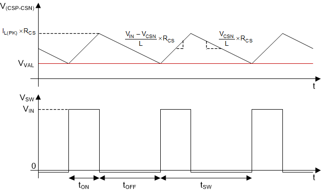
The following operating description of the TPS92519-Q1 refers to the Functional Block Diagram and the waveforms in Figure 7-1. The main control loop of the TPS92519-Q1 is based on an adaptive on-time pulse width modulation (PWM) technique that combines a constant on-time control with an inductor valley current sense circuit for pseudo-fixed frequency operation. This proprietary control technique enables closed-loop regulation of LED current and fast dynamic response necessary to meet the requirements for LED pixel control and LED matrix beam applications.
 Figure 7-1 Adaptive On Time Control Buck Converter Waveforms
In steady state, the high-side MOSFET is turned on at the beginning of each cycle. The on-time duration of this MOSFET is controlled by an internal one-shot timer and the high-side MOSFET is turned off after the timer expires. The one-shot timer duration is set by the output voltage measured at the CSP pin, VCSP, and the input voltage measured at the VIN pin, VIN, to maintain a pseudo-fixed frequency. During the on-time interval, the inductor current increases with a slope proportional to the voltage applied across its terminals (VIN – VCSP).
The low-side MOSFET is turned on after a fixed deadtime and the inductor current then decreases with the constant slope proportional to the output voltage, VCSP. Inductor current measured by the external sense resistor is compared to the valley threshold, VVAL, by an internal high-speed comparator. This MOSFET is turned off and the one-shot timer is initiated when the sensed inductor current falls below the valley threshold voltage. The high-side MOSFET is turned on again after a fixed deadtime.
The internal rail-to-rail error amplifier sets the valley threshold voltage and regulates the average inductor current based on a reference set by IADJx input. A simple integral loop compensation circuit consisting of a capacitor connected from the COMP pin to GND provides a stable and high-bandwidth response. As the inductor current is directly sensed by an external resistor, the device operation is not sensitive to the ESR of the output capacitors and is compatible with common multi-layered ceramic capacitors (MLCC).