SNVS900B DECEMBER 2012 – December 2015 TPS92560
PRODUCTION DATA.
- 1 Features
- 2 Applications
- 3 Description
- 4 Revision History
- 5 Pin Configuration and Functions
- 6 Specifications
- 7 Detailed Description
- 8 Application and Implementation
- 9 Power Supply Recommendations
- 10Layout
- 11Device and Documentation Support
- 12Mechanical, Packaging, and Orderable Information
Package Options
Mechanical Data (Package|Pins)
- DGQ|10
Thermal pad, mechanical data (Package|Pins)
- DGQ|10
Orderable Information
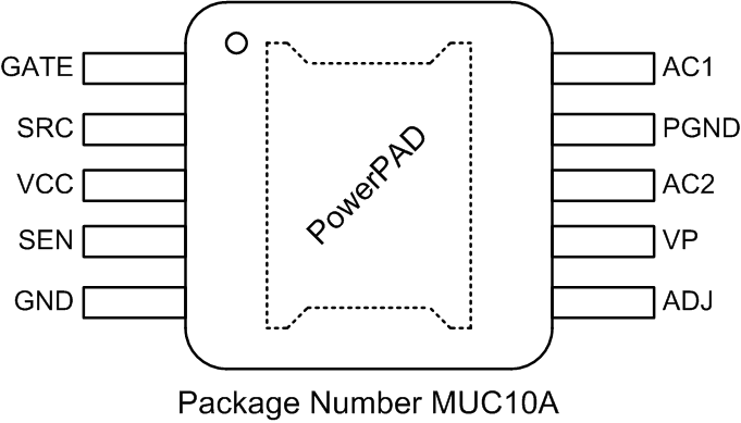
5 Pin Configuration and Functions
DGQ Package
10-Pin HVSSOP
Top View

Pin Functions
| PIN | I/O | DESCRIPTION | APPLICATION INFORMATION | |
|---|---|---|---|---|
| NO. | NAME | |||
| 1 | GATE | O | Gate driver output pin | Connect to the Gate terminal of the low-side N-channel Power FET |
| 2 | SRC | I | Gate driver return | Connect to the Source terminal of the low-side N-channel Power FET |
| 3 | VCC | O | VCC regulator output | Connect 0.47-μF decoupling capacitor from this pin to SRC pin |
| 4 | SEN | I | Current sense pin | Kelvin-sense current sensing input. Should connect to the current sensing resistor, RSEN. |
| 5 | GND | — | Analog ground | Reference point for current sensing. |
| 6 | ADJ | I | LED current adjust pin | Connect to resistor divider from LED top voltage rail to set LED current |
| 7 | VP | I | Power supply of the IC | Connect it to the LED top voltage rail (for boost) or Connect it through a diode from LED top voltage rail (for SEPIC) |
| 8 | AC2 | I | Power return terminal | Connect to AC or DC input terminal |
| 9 | PGND | — | Power ground | Connect to system ground plane |
| 10 | AC1 | I | Power return terminal | Connect to AC or DC input terminal |
| PowerPAD™ | — | Thermal DAP | Connect to system ground plane for heat dissipation | |