SLVSC76E February   2014  – May 2018 TPS92630-Q1

PRODUCTION DATA.  

  1. Features
  2. Applications
  3. Description
  4. Typical Application Schematic
  5. Revision History
  6. Description (Continued)
  7. Pin Configuration and Functions
    1.     Pin Functions
  8. Specifications
    1. 8.1 Absolute Maximum Ratings
    2. 8.2 ESD Ratings
    3. 8.3 Recommended Operating Conditions
    4. 8.4 Thermal Information
    5. 8.5 Electrical Characteristics
    6. 8.6 Timing Requirements
    7. 8.7 Typical Characteristics
  9. Parameter Measurement Information
  10. 10Detailed Description
    1. 10.1 Overview
    2. 10.2 Functional Block Diagram
    3. 10.3 Feature Description
      1. 10.3.1 Constant LED-Current Setting
      2. 10.3.2 PWM Control
      3. 10.3.3 FAULT Diagnostics
      4. 10.3.4 Short-Circuit Detection
      5. 10.3.5 Open-Load Detection
      6. 10.3.6 Thermal Foldback
    4. 10.4 Device Functional Modes
      1. 10.4.1 Thermal Information
      2. 10.4.2 Operation With V(VIN) < 5 V (Minimum V(VIN))
      3. 10.4.3 Operation With 5 V < V(VIN) < 9 V (Lower-Than-Normal Automotive Battery Voltage)
  11. 11Applications and Implementation
    1. 11.1 Application Information
    2. 11.2 Typical Applications
      1. 11.2.1 Stoplight and Taillight Application With PWM Generator
        1. 11.2.1.1 Design Requirements
        2. 11.2.1.2 Detailed Design Procedure
          1. 11.2.1.2.1 Step-by-Step Design Procedure
            1. 11.2.1.2.1.1 R(REF)
            2. 11.2.1.2.1.2 Duty Cycle
            3. 11.2.1.2.1.3 Input and Output Capacitors
        3. 11.2.1.3 PWM Dimming Application Curve
      2. 11.2.2 Simple Stop-Light and Taillight Application
        1. 11.2.2.1 Design Requirements
        2. 11.2.2.2 Detailed Design Procedure
          1. 11.2.2.2.1 Step-by-Step Design Procedure
            1. 11.2.2.2.1.1 R(REF)
            2. 11.2.2.2.1.2 R(Stop)
            3. 11.2.2.2.1.3 Input and Output Capacitors
      3. 11.2.3 Parallel Connection
        1. 11.2.3.1 Design Requirements
        2. 11.2.3.2 Detailed Design Procedure
          1. 11.2.3.2.1 Step-by-Step Design Procedure
            1. 11.2.3.2.1.1 R(REF)
            2. 11.2.3.2.1.2 Input and Output Capacitors
      4. 11.2.4 Alternate Parallel Connection
        1. 11.2.4.1 Design Requirements
        2. 11.2.4.2 Detailed Design Procedure
          1. 11.2.4.2.1 Step-by-Step Design Procedure
            1. 11.2.4.2.1.1 R(REF)
            2. 11.2.4.2.1.2 Input and Output Capacitors
      5. 11.2.5 High-Side PWM Dimming
        1. 11.2.5.1 Design Requirements
        2. 11.2.5.2 Detailed Design Procedure
          1. 11.2.5.2.1 Step-by-Step Design Procedure
            1. 11.2.5.2.1.1 Ratio of Resistors, R1 / R2
            2. 11.2.5.2.1.2 R1 and R2 Selection
            3. 11.2.5.2.1.3 Input and Output Capacitors
  12. 12Power Supply Recommendations
  13. 13Layout
    1. 13.1 Layout Guidelines
    2. 13.2 Layout Example
  14. 14Device and Documentation Support
    1. 14.1 Documentation Support
      1. 14.1.1 Related Documentation
    2. 14.2 Receiving Notification of Documentation Updates
    3. 14.3 Community Resources
    4. 14.4 Trademarks
    5. 14.5 Electrostatic Discharge Caution
    6. 14.6 Glossary
  15. 15Mechanical, Packaging, and Orderable Information

Package Options

Mechanical Data (Package|Pins)
Thermal pad, mechanical data (Package|Pins)
Orderable Information

Constant LED-Current Setting

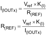
Control of the three LED output channels is through separate linear current regulators. A common external resistor sets the current in each channel. The device also features two current levels with external circuitry, intended for stop- and tail-light applications.

See Equation 1 on how to set the current:

Equation 1. TPS92630-Q1 eq1_Ioutx_slvsc76.gif