SNVS902A October 2012 – October 2015 TPS92640 , TPS92641
PRODUCTION DATA.
- 1 Features
- 2 Applications
- 3 Description
- 4 Revision History
- 5 Pin Configuration and Functions
- 6 Specifications
-
7 Detailed Description
- 7.1 Overview
- 7.2 Functional Block Diagram
- 7.3
Feature Description
- 7.3.1 Controlled On-Time Architecture
- 7.3.2 Switching Frequency
- 7.3.3 Average LED Current
- 7.3.4 Analog Dimming and True-Zero Operation
- 7.3.5 Undervoltage Lockout (UVLO)
- 7.3.6 PWM Dimming Using the UDIM Pin
- 7.3.7 External Shunt FET PWM Dimming
- 7.3.8 VCC Regulation and Start-up
- 7.3.9 Precision Reference
- 7.3.10 Control Loop Compensation
- 7.3.11 Overcurrent Protection
- 7.3.12 Overvoltage Protection (OVP)
- 7.3.13 Boot Undervoltage Lockout (UVLO)
- 7.4 Device Functional Modes
-
8 Application and Implementation
- 8.1 Application Information
- 8.2
Typical Applications
- 8.2.1
TPS92640: Design Procedure
- 8.2.1.1 Design Requirements
- 8.2.1.2
Detailed Design Procedure
- 8.2.1.2.1 Set Output Voltage Feedback Ratio
- 8.2.1.2.2 Set Switching Frequency
- 8.2.1.2.3 Set Average LED Current
- 8.2.1.2.4 Set Inductor Ripple Current
- 8.2.1.2.5 Set LED Ripple Current and Determine Output Capacitance, COUT
- 8.2.1.2.6 Choose N-Channel MOSFETs
- 8.2.1.2.7 Choose Input Capacitance
- 8.2.1.2.8 Set the Turnon Voltage and Undervoltage Lockout Hysteresis
- 8.2.2
TPS92640 - PWM Dimming Application
- 8.2.2.1 Design Requirements
- 8.2.2.2
Detailed Design Procedure
- 8.2.2.2.1 Calculate Operating Points
- 8.2.2.2.2 Output Voltage Feedback
- 8.2.2.2.3 Switching Frequency
- 8.2.2.2.4 Set the Feedback Reference and LED Current
- 8.2.2.2.5 Calculate the Inductor Value
- 8.2.2.2.6 Calculate the Output Capacitor Value
- 8.2.2.2.7 Calculate the MOSFET Parameters
- 8.2.2.2.8 Calculate the Minimum Input Capacitance
- 8.2.2.2.9 Undervoltage Lockout and Hysteresis
- 8.2.2.3 Application Curve
- 8.2.1
TPS92640: Design Procedure
- 9 Power Supply Recommendations
- 10Layout
- 11Device and Documentation Support
- 12Mechanical, Packaging, and Orderable Information
Package Options
Mechanical Data (Package|Pins)
- PWP|16
Thermal pad, mechanical data (Package|Pins)
- PWP|16
Orderable Information
10 Layout
10.1 Layout Guidelines
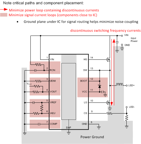
The performance of any switching converter depends as much upon the layout of the PCB as the component selection. Following a few simple guidelines will maximize noise rejection and minimize the generation of EMI within the circuit.
Discontinuous currents are the most likely to generate EMI, therefore take care when routing these paths. The main path for discontinuous current in the TPS92640 and TPS92641 buck converters contain the input capacitor (CIN), the low side MOSFET (QLS), and the high side MOSFET (QHS). This loop should be kept as small as possible and the connections between all three components should be short and thick to minimize parasitic inductance. In particular, the switch node (where L, QLS and QHS connect) should be just large enough to connect the components without excessive heating from the current it carries. The current sense trace (CS pin) should be run along with a ground plane or have differential traces run for CS and ground.
In some applications, the LED or LED array can be far away (several inches or more) from the circuit, or on a separate PCB connected by a wiring harness. When an output capacitor is used and the LED array is large or separated from the rest of the converter, the output capacitor should be placed close to the LEDs to reduce the effects of parasitic inductance on the AC impedance of the capacitor.
10.2 Layout Example
 Figure 26. Layout Recommendation
10.3 EMI and Noise Considerations
In synchronous rectifier, the high speed gate drive signals can generate significant conducted and radiated EMI. This noise can couple with high impedance nodes of the IC and result in undesirable operation. A small (4 Ω to 10 Ω) resistors, RHG and RLG, in series with the gate drive signals are recommended to slow the slew-rate of the SW node and reduce the noise signature. They also improve the robustness of the circuit by reducing the noise coupling in to sensitive nodes such as UDIM, CS, RON and IADJ.
In other to further reduce EMI signature, good PCB layout techniques must be implemented. The loop area between the synchronous NFET, inductor and output capacitor should be minimized to reduce radiated EMI due to switching action. The trace lengths of high impedance nodes (UDIM, CS, RON and IADJ) should be minimized and shielded from switching noise. The parasitic capacitance between switching node and ground node should be minimized to reduce common mode noise. Other common layout techniques such as star ground and noise suppression using local bypass capacitors should be followed to maximize noise rejection and minimize EMI within the circuit.