SLVSDD9 March 2017 TPS92692 , TPS92692-Q1
PRODUCTION DATA.
- 1 Features
- 2 Applications
- 3 Description
- 4 Revision History
- 5 Pin Configuration and Functions
- 6 Specifications
-
7 Detailed Description
- 7.1 Overview
- 7.2 Functional Block Diagram
- 7.3
Feature Description
- 7.3.1 Internal Regulator and Undervoltage Lockout (UVLO)
- 7.3.2 Oscillator
- 7.3.3 Spread Spectrum Frequency Modulation
- 7.3.4 Gate Driver
- 7.3.5 Rail-to-Rail Current Sense Amplifier
- 7.3.6 Transconductance Error Amplifier
- 7.3.7 Switch Current Sense
- 7.3.8 Slope Compensation
- 7.3.9 Analog Adjust Input
- 7.3.10 DIM/PWM Input
- 7.3.11 Series P-Channel FET Dimming Gate Driver Output
- 7.3.12 Soft-Start
- 7.3.13 Current Monitor Output
- 7.3.14 Output Overvoltage Protection
- 7.3.15 Output Short-circuit Protection
- 7.3.16 Thermal Protection
- 7.3.17 Fault Indicator (FLT)
- 7.4 Device Functional Modes
-
8 Application and Implementation
- 8.1
Application Information
- 8.1.1 Duty Cycle Considerations
- 8.1.2 Inductor Selection
- 8.1.3 Output Capacitor Selection
- 8.1.4 Input Capacitor Selection
- 8.1.5 Main Power MOSFET Selection
- 8.1.6 Rectifier Diode Selection
- 8.1.7 LED Current Programming
- 8.1.8 Switch Current Sense Resistor
- 8.1.9 Slope Compensation
- 8.1.10 Feedback Compensation
- 8.1.11 Soft-Start
- 8.1.12 Overvoltage and Undervoltage Protection
- 8.1.13 Analog to PWM Dimming Considerations
- 8.1.14 Direct PWM Dimming Considerations
- 8.1.15 Series P-Channel MOSFET Selection
- 8.2
Typical Applications
- 8.2.1
Typical Boost LED Driver
- 8.2.1.1 Design Requirements
- 8.2.1.2
Detailed Design Procedure
- 8.2.1.2.1 Calculating Duty Cycle
- 8.2.1.2.2 Setting Switching Frequency
- 8.2.1.2.3 Setting Dither Modulation Frequency
- 8.2.1.2.4 Inductor Selection
- 8.2.1.2.5 Output Capacitor Selection
- 8.2.1.2.6 Input Capacitor Selection
- 8.2.1.2.7 Main N-Channel MOSFET Selection
- 8.2.1.2.8 Rectifying Diode Selection
- 8.2.1.2.9 Programming LED Current
- 8.2.1.2.10 Setting Switch Current Limit
- 8.2.1.2.11 Programming Slope Compensation
- 8.2.1.2.12 Deriving Compensator Parameters
- 8.2.1.2.13 Setting Start-up Duration
- 8.2.1.2.14 Setting Overvoltage Protection Threshold
- 8.2.1.2.15 Analog-to-PWM Dimming Considerations
- 8.2.1.3 Application Curves
- 8.2.2
Typical Buck-Boost LED Driver
- 8.2.2.1 Design Requirements
- 8.2.2.2
Detailed Design Procedure
- 8.2.2.2.1 Calculating Duty Cycle
- 8.2.2.2.2 Setting Switching Frequency
- 8.2.2.2.3 Setting Dither Modulation Frequency
- 8.2.2.2.4 Inductor Selection
- 8.2.2.2.5 Output Capacitor Selection
- 8.2.2.2.6 Input Capacitor Selection
- 8.2.2.2.7 Main N-Channel MOSFET Selection
- 8.2.2.2.8 Rectifier Diode Selection
- 8.2.2.2.9 Programming LED Current
- 8.2.2.2.10 Setting Switch Current Limit and Slope Compensation
- 8.2.2.2.11 Programming Slope Compensation
- 8.2.2.2.12 Deriving Compensator Parameters
- 8.2.2.2.13 Setting Startup Duration
- 8.2.2.2.14 Setting Overvoltage Protection Threshold
- 8.2.2.2.15 Direct PWM Dimming Consideration
- 8.2.2.3 Application Curves
- 8.2.1
Typical Boost LED Driver
- 8.1
Application Information
- 9 Power Supply Recommendations
- 10Layout
- 11Device and Documentation Support
- 12Mechanical, Packaging, and Orderable Information
Package Options
Mechanical Data (Package|Pins)
- PWP|20
Thermal pad, mechanical data (Package|Pins)
- PWP|20
Orderable Information
8 Application and Implementation
NOTE
Information in the following applications sections is not part of the TI component specification, and TI does not warrant its accuracy or completeness. TI’s customers are responsible for determining suitability of components for their purposes. Customers should validate and test their design implementation to confirm system functionality.
8.1 Application Information
The TPS92692 and TPS92692-Q1 controllers are suitable for implementing step-up or step-down LED driver topologies including boost, buck-boost, SEPIC, and flyback. Use the following design procedure to select component values for the TPS92692-Q1 device. This section presents a simplified discussion of the design process for the boost and buck-boost converter. The expressions derived for the buck-boost topology can be altered to select components for a 1:1 coupled-inductor SEPIC converter. The design procedure can be easily adapted for flyback and similar converter topologies.
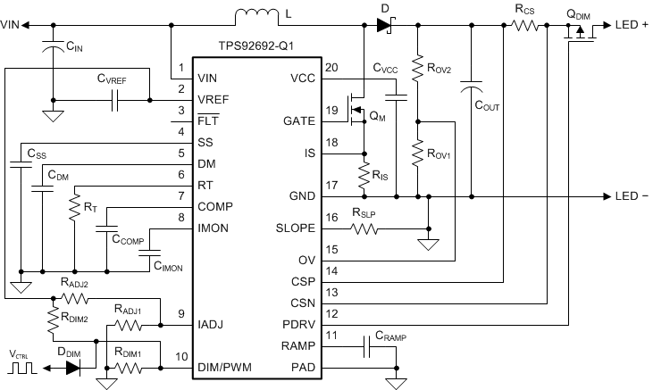 Figure 36. Boost LED Driver
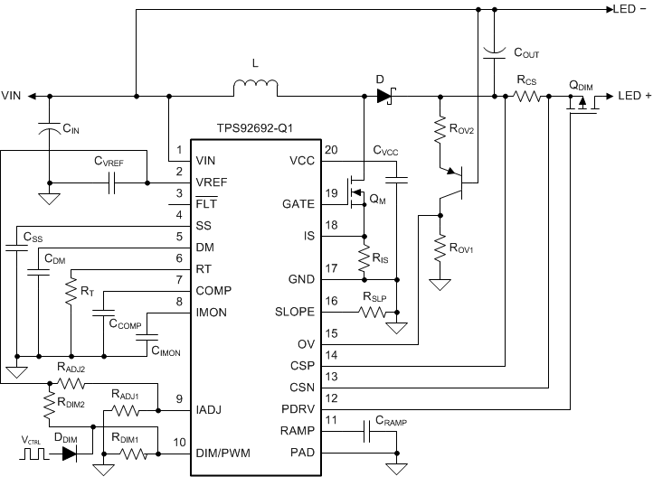 Figure 37. Buck-Boost LED Driver
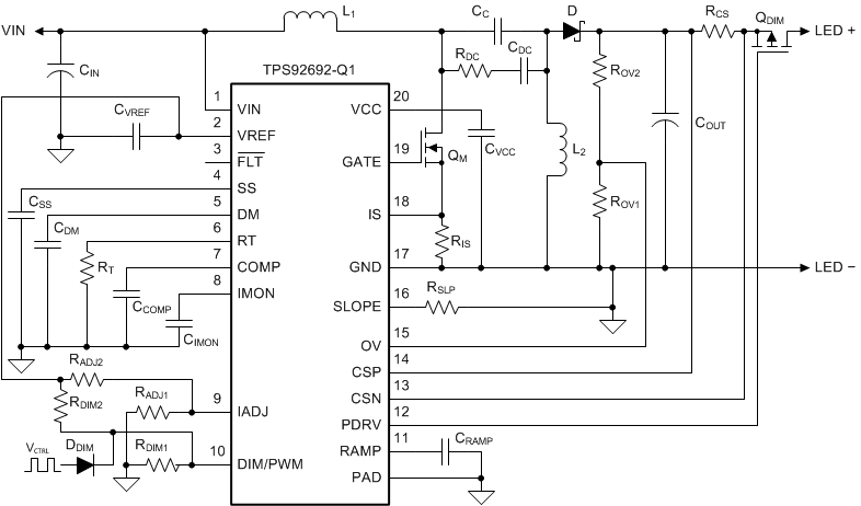 Figure 38. SEPIC LED Driver
8.1.1 Duty Cycle Considerations
The switch duty cycle, D, defines the converter operation and is a function of the input and output voltages. In steady state, the duty cycle is derived using expression:
Boost:

Buck-Boost:

The minimum duty cycle, DMIN, and maximum duty cycle, DMAX, are calculated by substituting maximum input voltage, VIN(MAX), and the minimum input voltage, VIN(MIN), respectively in the previous expressions. The minimum duty cycle achievable by the device is determined by the leading edge blanking period and the switching frequency. The maximum duty cycle is limited by the internal oscillator to 90% (typ) to allow for minimum off-time. It is necessary for the operating duty cycle to be within the operating limits of the device to ensure closed-loop LED current regulation over the specified input and output voltage range.
8.1.2 Inductor Selection
The choice of inductor sets the continuous conduction mode (CCM) and discontinuous conduction mode (DCM) boundary condition. Therefore, one approach of selecting the inductor value is by deriving the relationship between the output power corresponding to CCM-DCM boundary condition, PO(BDRY) and inductance, L. This approach ensures CCM operation in battery-powered LED driver applications that are required to support different LED string configurations with a wide range of programmable LED current set points. The CCM-DCM boundary condition can be estimated either based on the lowest LED current and the lowest output voltage requirements for a given application or as a fraction of maximum output power, PO(MAX).


Boost:

Buck-Boost:

Select inductor with saturation current rating greater than the peak inductor current, IL(PK), at the maximum operating temperature.
Boost:

Buck-Boost:

8.1.3 Output Capacitor Selection
The output capacitors are required to attenuate the discontinuous or large ripple current generated by switching and achieve the desired peak-to-peak LED current ripple, ΔiLED(PP). The capacitor value depends on the total series resistance of the LED string, rD and the switching frequency, ƒSW.The capacitance required for the target LED ripple current can be calculated based on following equations.
Boost:

Buck-Boost:

When choosing the output capacitors, it is important to consider the ESR and the ESL characteristics as they directly impact the LED current ripple. Ceramic capacitors are the best choice due to their low ESR, high ripple current rating, long lifetime, and good temperature performance. When selecting ceramic capacitors, it is important to consider the derating factors associated with higher temperature and DC bias operating conditions. TI recommends an X7R dielectric with voltage rating greater than maximum LED stack voltage. An aluminum electrolytic capacitor can be used in parallel with ceramic capacitors to provide bulk energy storage. The aluminum capacitors must have necessary RMS current and temperature ratings to ensure prolonged operating lifetime. The minimum allowable RMS output capacitor current rating, ICOUT(RMS), can be approximated:
Boost and Buck-Boost:

8.1.4 Input Capacitor Selection
The input capacitors, CIN, smooth the input voltage ripple and store energy to supply input current during input voltage or PWM dimming transients. The series inductor in the Boost and SEPIC topologies provides continuous input current and requires a smaller input capacitor to achieve desired input ripple voltage, ΔvIN(PP). The Buck-Boost and Flyback topologies have discontinuous input current and require a larger capacitor to achieve the same input voltage ripple. Based on the switching frequency, ƒSW, and the maximum duty cycle, DMAX, the input capacitor value can be calculated as follows:
Boost:

Buck-Boost:

X7R dielectric-based ceramic capacitors are the best choice due to their low ESR, high ripple current rating, and good temperature performance. For applications using PWM dimming, TI recommends an aluminum electrolytic capacitor in addition to ceramic capacitors to minimize the voltage deviation due to large input current transients generated in conjunction with the rising and falling edges of the LED current.
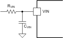 Figure 39. VIN Filter
Decouple VIN pin with a 0.1-µF ceramic capacitor, placed as close as possible to the device and a series 10-Ω resistor to create a 150-kHz low-pass filter.
8.1.5 Main Power MOSFET Selection
The power MOSFET is required to sustain the maximum switch node voltage, VSW, and switch RMS current derived based on the converter topology. TI recommends a drain voltage VDS rating of at least 10% greater than the maximum switch node voltage to ensure safe operation. The MOSFET drain-to-source breakdown voltage, VDS, is calculated using the following expressions.
Boost:

Buck-Boost:

The voltage, VO(OV), is the overvoltage protection threshold and the worst-case output voltage under fault conditions. The worst case MOSFET RMS current for Boost and Buck-Boost topology is dependent on maximum output power, PO(MAX), and is calculated as follows:

Select a MOSFET with low total gate charge, Qg, to minimize gate drive and switching losses. The MOSFET RDS resistance is usually a less critical parameter because the switch conduction losses are not a significant part of the total converter losses at high operating frequencies. The switching and conduction losses are calculated as follows:


CRSS is the MOSFET reverse transfer capacitance. IL is the average inductor current. IGATE is gate drive output current, typically 500 mA. The MOSFET power rating and package is selected based on the total calculated loss, the ambient operating temperature, and maximum allowable temperature rise.
8.1.6 Rectifier Diode Selection
A Schottky diode (when used as a rectifier) provides the best efficiency due to its low forward voltage drop and near-zero reverse recovery time. TI recommends a diode with a reverse breakdown voltage, VD(BR), greater than or equal to MOSFET drain-to-source voltage, VDS, for reliable performance. It is important to understand the leakage current characteristics of the Schottky diode, especially at high operating temperatures because it impacts the overall converter operation and efficiency.
Use Equation 27 to calculate the current through the diode, ID.

The diode power rating and package is selected based on the calculated current, the ambient temperature and the maximum allowable temperature rise.
8.1.7 LED Current Programming
The LED current is set by the external current sense resistor, RCS, and the analog adjust voltage, VIADJ. The current sense resistor is placed in series with the LED load. The CSP and CSN inputs of the internal rail-to-rail current sense amplifier are connected to the RCS resistor to enable closed-loop regulation. When VIADJ > 2.5 V, the internal 2.4-V reference sets the V(CSP-CSN) threshold to 170.7 mV and the LED current is regulated to:

The LED current can be programmed by varying VIADJ between 140 mV to 2.25 V. The LED current can be calculated using:

TI recommends a low-pass common-mode filter consisting of 10-Ω resistors in series with CSP and CSN inputs and 0.01-µF capacitors to ground to minimize the impact of voltage ripple and noise on LED current accuracy (see Figure 24 section). A 0.1-µF capacitor across CSP and CSN is included to filter high-frequency differential noise.
8.1.8 Switch Current Sense Resistor
The switch current sense resistor, RIS, is used to implement peak current mode control and to set the peak switch current limit. The value of RIS is selected to protect the main switching MOSFET under fault conditions. The RIS can be calculated based on peak inductor current, iL(PK), and switch current limit threshold, VIS(LIMIT).

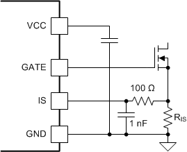 Figure 40. IS Input Filter
The use of a 1-nF and 100-Ω low-pass filter is optional. If used, the recommended resistor value is less than 500 Ω in order to limit its influence on the internal slope compensation signal.
8.1.9 Slope Compensation
The magnitude of internal artificial ramp, VSL, is set by slope resistor RSLP. The device compensates for the changes in input voltage, VIN and output voltage sensed by CSP pin, VCSP to achieve stable inner current loop operation over wide range of operating conditions. The value of RSLP is determined by the inductor, L and the switch current sense resistor, RIS and is independent of input and output voltage for Boost, Boost-to-Battery and Buck-Boost topologies.

8.1.10 Feedback Compensation
The open-loop response is the product of the modulator transfer function (shown in Equation 32) and the feedback transfer function. Using a first-order approximation, the modulator transfer function can be modeled as a single pole created by the output capacitor, and in the boost and buck-boost topologies, a right half-plane zero created by the inductor, where both have a dependence on the LED string dynamic resistance, rD. The ESR of the output capacitor is neglected in the analysis. The small-signal modulator model also includes a DC gain factor that is dependent on the duty cycle, output voltage, and LED current.

The Table 2 summarizes the expression for the small-signal model parameters.
Table 2. Small-Signal Model Parameters
| DC GAIN (G0) | POLE FREQUENCY (ωP) | ZERO FREQUENCY (ωZ) | |
|---|---|---|---|
| Boost |  |
 |
 |
| Buck-Boost |  |
 |
 |
The feedback transfer function includes the current sense resistor and the loop compensation of the transconductance amplifier. A compensation network at the output of the error amplifier is used to configure loop gain and phase characteristics. A simple capacitor, CCOMP, from COMP to GND (as shown in Figure 41) provides integral compensation and creates a pole at the origin. Alternatively, a network of RCOMP, CCOMP, and CHF, shown in Figure 42, can be used to implement proportional and integral (PI) compensation to create a pole at the origin, a low-frequency zero, and a high-frequency pole.
The feedback transfer function is defined as follows.
Feedback transfer function with integral compensation:

Feedback transfer function with proportional integral compensation:

The pole at the origin minimizes output steady-state error. High bandwidth is achieved with the PI compensator by placing the low-frequency zero an order of magnitude less than the crossover frequency. Use the following expressions to calculate the compensation network.
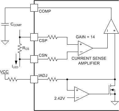 Figure 41. Integral Compensator
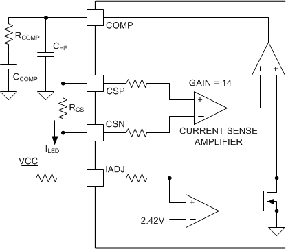 Figure 42. Proportional Integral Compensator
Boost and Buck-Boost with integral compensator:

Boost and Buck-Boost with proportional integral compensator:


The loop response is verified by applying step input voltage transients. The goal is to minimize LED current overshoot and undershoot with a damped response. Additional tuning of the compensation network may be necessary to optimize PWM dimming performance.
8.1.11 Soft-Start
The soft-start time (tSS) is the time required for the LED current to reach the target set point. The required soft-start time is programmed using a capacitor, CSS, from SS pin to GND, and is based on the LED current, output capacitor, and output voltage.

8.1.12 Overvoltage and Undervoltage Protection
The overvoltage threshold is programmed using a resistor divider, ROV2 and ROV1, from the output voltage, VO, to GND for Boost and SEPIC topologies, as shown in Figure 36 and Figure 38. If the LEDs are referenced to a potential other than GND, as in the Buck-Boost, the output voltage is sensed and translated to ground by using a PNP transistor and level-shift resistors, as shown in Figure 37. The overvoltage turn-off threshold, VO(OV), is:
Boost:

Buck and Buck-Boost:

The overvoltage hysteresis, VOV(HYS) is:

The corresponding undervoltage fault threshold, VO(UV) is:

8.1.13 Analog to PWM Dimming Considerations
The analog to PWM duty cycle translation is based on the internal PWM generator, configured by connecting a capacitor across RAMP pin and GND, as shown in Figure 29. The minimum PWM duty cycle is programmed by setting the voltage on DIM/PWM pin, VDIM using a resistor divider from VREF pin to GND.


The device is designed to support a minimum PWM duty cycle of 4% with better than 5% accuracy from DIM/PWM input to PDRV output in this operating mode. To avoid excess loading of the VREF LDO output, TI recommends a resistor network with sum of resistors RDIM1 and RDIM2 greater than 10 kΩ. A bypass capacitor of 0.1-µF prevents noise coupling and improves performs for low dimming values.
8.1.14 Direct PWM Dimming Considerations
The device can be configured to implement dimming function based on external PWM command by disabling the internal ramp generator, as explained in DIM/PWM Input section. The internal comparator reference is set to 2.49 V by connecting a 249-kΩ resistor, RRAMP, from the RAMP pin to GND. The internal PWM duty cycle is controlled by an external 5-V or 3.3-V signal, generated by a command module or a microcontroller.
8.1.15 Series P-Channel MOSFET Selection
When PWM dimming, the device requires another P-channel MOSFET placed in series with the LED load. Select a P-channel MOSFET with gate-to-source voltage rating of 10-V or higher and with a drain-to-source breakdown voltage rating greater than the output voltage. Ensure that the drain current rating of the P-channel MOSFET exceeds the programmed LED current by at least 10%.
It is important to consider the FET input capacitance and on-resistance as it impacts the accuracy and efficiency of the LED driver. TI recommends a FET with lower input capacitance and gate charge to minimize the errors caused by rise and fall times when PWM dimming at low duty cycles.
8.2 Typical Applications
8.2.1 Typical Boost LED Driver
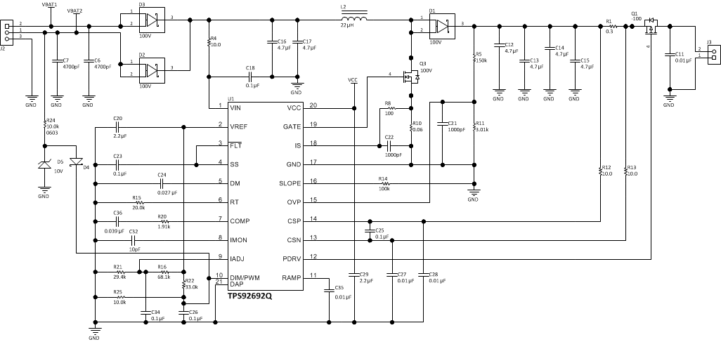 Figure 43. Boost LED Driver With High-Side Current Sense
8.2.1.1 Design Requirements
Table 3 shows the design parameters for the boost LED driver application.
Table 3. Design Parameters
| PARAMETER | TEST CONDITIONS | MIN | TYP | MAX | UNIT | |
|---|---|---|---|---|---|---|
| INPUT CHARACTERISTICS | ||||||
| Input voltage range | 7 | 14 | 18 | V | ||
| Input UVLO setting | 4.5 | V | ||||
| OUTPUT CHARACTERISTICS | ||||||
| LED forward voltage | 2.8 | 3.2 | 3.6 | V | ||
| Number of LEDs in series | 14 | |||||
| VO | Output voltage | LED+ to LED– | 39.2 | 44.8 | 50.4 | V |
| ILED | Output current | 350 | 500 | mA | ||
| RR | LED current ripple ratio | 4% | ||||
| rD | LED string resistance | 3 | Ω | |||
| PO(MAX) | Maximum output power | 25 | W | |||
| fPWM | PWM dimming frequency | 240 | Hz | |||
| DPWM | Analog to PWM duty cycle set point (low brightness mode) | 8 | % | |||
| SYSTEMS CHARACTERISTICS | ||||||
| PO(BDRY) | Output power at CCM-DCM boundary condition | 6 | W | |||
| ΔvIN(PP) | Input voltage ripple | 20 | mV | |||
| VO(OV) | Output overvoltage protection threshold | 62 | V | |||
| VOV(HYS) | Output overvoltage protection hysteresis | 3 | V | |||
| tss | Soft-start period | 8 | ms | |||
| fDM | Dither Modulation Frequency | 600 | Hz | |||
| fSW | Switching frequency | 390 | kHz | |||
8.2.1.2 Detailed Design Procedure
This procedure is for the boost LED driver application.
8.2.1.2.1 Calculating Duty Cycle
Solve for D, DMAX, and DMIN:


8.2.1.2.2 Setting Switching Frequency
Solve for RT:

The closest standard resistor of 20 kΩ is selected.
8.2.1.2.3 Setting Dither Modulation Frequency
Solve for CDM:

The closest standard capacitor is 27 nF.
8.2.1.2.4 Inductor Selection
The inductor is selected to meet the CCM-DCM boundary power requirement, PO(BDRY). In most applications, PO(BDRY) is set to be 1/3 of the maximum output power, PO(MAX). The inductor value is calculated for typical input voltage, VIN(TYP), and output voltage, VO(TYP):

The closest standard inductor is 22 µH.
For best results, ensure that the inductor saturation current rating is greater than the peak inductor current, IL(PK).

8.2.1.2.5 Output Capacitor Selection
The specified peak-to-peak LED current ripple, ΔiLED(PP), is:

The output capacitance required to achieve the target LED current ripple is:

Four 4.7-µF, 100-V rated X7R ceramic capacitors are used in parallel to achieve a combined output capacitance of 18.8 µF.
8.2.1.2.6 Input Capacitor Selection
The input capacitor is required to reduce switching noise conducted through the input wires and reduced the input impedance of the LED driver. The capacitor required to limit peak-to-peak input ripple voltage ripple, ΔvIN(PP), to 20 mV is given by:

Two 4.7-µF, 50-V X7R ceramic capacitors are used in parallel to achieve a combined input capacitance of 9.4-µF.
8.2.1.2.7 Main N-Channel MOSFET Selection
Ensure that the MOSFET ratings exceed the maximum output voltage and RMS switch current.


A N-channel MOSFET with a voltage rating of 100-V and a current rating of 4 A is required for this design.
8.2.1.2.8 Rectifying Diode Selection
Select a diode should be selected based on the following voltage and current ratings:


A 100-V Schottky diode with low reverse leakage current is suitable for this design. The package must be able to handle the power dissipation resulting from continuous forward current, ID, of 0.5 A.
8.2.1.2.9 Programming LED Current
The LED current can be programmed to match the LED string configuration by using a resistor divider, RADJ1 and RADJ2, from VREF to GND for a given sense resistor, RCS, as shown in Figure 43. To maximize the accuracy, the IADJ pin voltage is set to 2.1 V for the specified maximum LED current of 500-mA. The current sense resistor, RCS, is then calculated as:

A standard resistor of 0.3 Ω is selected. Table 4 summarizes the IADJ pin voltage and the choice of the RADJ1 and RADJ2 resistors for different current settings.
Table 4. Design Requirements
| LED CURRENT | IADJ VOLTAGE (VIADJ) | RADJ1 | RADJ2 |
|---|---|---|---|
| 100 mA | 420 mV | 6.34 kΩ | 68.1 kΩ |
| 350 mA | 1.47 V | 29.4 kΩ | 68.1 kΩ |
| 500 mA | 2.1 V | 49.9 kΩ | 68.1 kΩ |
8.2.1.2.10 Setting Switch Current Limit
Solve for current sense resistor, RIS:

A standard value of 0.06 Ω is selected.
8.2.1.2.11 Programming Slope Compensation
The artificial slope is programmed by resistor, RSL.

A standard resistor of 100 kΩ is selected.
8.2.1.2.12 Deriving Compensator Parameters
The modulator transfer function for the Boost converter is derived for nominal VIN voltage and corresponding duty cycle, D, and is given by the following equation. (See Feedback Compensation section for more information.)

The proportional-integral compensator components CCOMP and RCOMP are obtained by solving the following expressions:


The closet standard capacitor of 18-nF and resistor of 4.12-kΩ is selected. The high frequency pole location is set by a 1-nF CHF capacitor.
8.2.1.2.13 Setting Start-up Duration
The soft-start capacitor required to achieve start-up in 8 ms is given by:

The closet standard capacitor of 100 nF is selected.
8.2.1.2.14 Setting Overvoltage Protection Threshold
The overvoltage protection threshold of 62 V and hysteresis of 3 V is set by the ROV1 and ROV2 resistor divider.


The standard resistor values of 150 kΩ and 3.01 kΩ are chosen.
8.2.1.2.15 Analog-to-PWM Dimming Considerations
The PWM dimming frequency is set by the CRAMP capacitor.

The closet standard capacitor of 10 nF is selected.
The PWM duty cycle of 8% programmed by setting the DIM/PWM voltage using resistor divider, RDIM1 and RDIM2 connected from VREF pin to GND.

The value of resistor, RDIM1 is set as of 10-kΩ. The resistor RDIM2 is calculated using the following equation:

A standard resistor of 33 kΩ is selected.
A P-channel MOSFET with a voltage rating of 100-V and a current rating of 1 A is required to enable series FET dimming for this design.
8.2.1.3 Application Curves
These curves are for the boost LED driver.
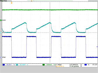
Ch2: Switch current sense voltage;
Ch4: LED current; Time: 1 µs/div
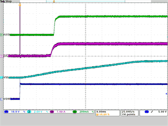
Ch3: Input current;
Ch4: LED current; Time: 4 ms/div
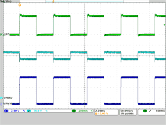
Ch2: PDRV voltage;
Ch4: LED current; Time: 2 ms/div
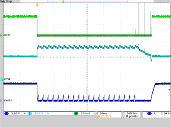
Ch2: CSP pin voltage;
Ch4: LED current; Time: 100 ms/div
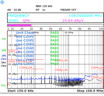 Figure 52. Conducted EMI Scan (SSFM Disabled)
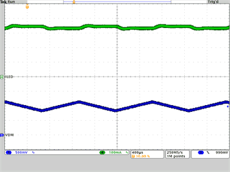
Ch4: LED current; Time: 400 µs/div
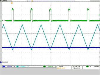
Ch2: RAMP pin voltage;
Ch4: LED current; Time: 2 ms/div
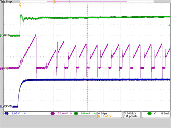
Ch3: Switch sense current resistor voltage;
Ch4: LED current; Time: 4 µs/div
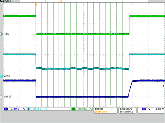
Ch2: CSP pin voltage;
Ch4: LED current; Time: 100 ms/div
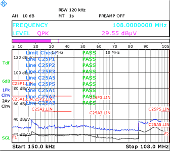 Figure 53. Conducted EMI Scan (SSFM Enabled)
8.2.2 Typical Buck-Boost LED Driver
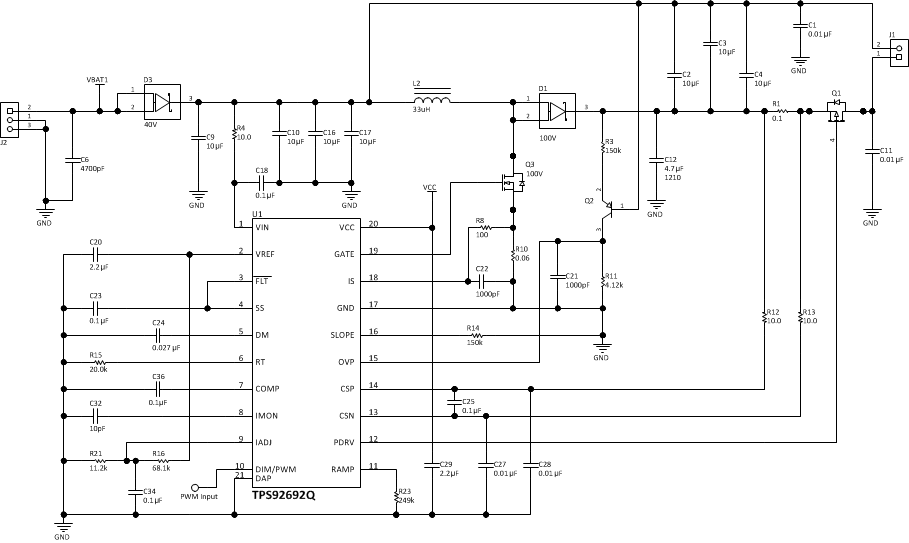 Figure 54. Buck-Boost LED Driver
8.2.2.1 Design Requirements
Buck-Boost LED drivers provide the flexibility needed in applications that support multiple LED load configurations. For such applications, it is necessary to modify the design procedure presented in to account for the wider range of output voltage and LED current specifications. This design is based on the maximum output power PO(MAX), set by the lumen output specified for the lighting application. The design procedure for a battery connected application with 3 to 9 LEDs in series and maximum 15 W output power is outlined in this section.
Table 5. Design Parameters
| PARAMETER | TEST CONDITIONS | MIN | TYP | MAX | UNIT | |
|---|---|---|---|---|---|---|
| INPUT CHARACTERISTICS | ||||||
| Input voltage range | 7 | 14 | 18 | V | ||
| Input UVLO setting | 4.5 | V | ||||
| OUTPUT CHARACTERISTICS | ||||||
| LED forward voltage | 2.8 | 3.2 | 3.6 | V | ||
| Number of LEDs in series | 3 | 7 | 11 | |||
| VO | Output voltage | LED+ to LED– | 8.4 | 22.4 | 39.6 | V |
| ILED | Output current | 100 | 500 | 1500 | mA | |
| ΔiLED(PP) | LED current ripple | 5% | ||||
| rD | LED string resistance | 0.9 | 2.1 | 3.3 | Ω | |
| PO(MAX) | Maximum output power | 12.6 | W | |||
| DPWM | Direct PWM dimming range | fPWM = 240 Hz | 4% | 100% | ||
| SYSTEMS CHARACTERISTICS | ||||||
| PO(BDRY) | Output power at CCM-DCM boundary condition | 3 | W | |||
| ΔvIN(PP) | Input voltage ripple | 70 | mV | |||
| VO(OV) | Output overvoltage protection threshold | 45 | V | |||
| VOV(HYS) | Output overvoltage protection hysteresis | 3 | V | |||
| tSS | Soft-start period | 8 | ms | |||
| fSW | Switching frequency | 390 | kHz | |||
8.2.2.2 Detailed Design Procedure
8.2.2.2.1 Calculating Duty Cycle
Solving for D, DMAX, and DMIN:


8.2.2.2.2 Setting Switching Frequency
Solving for RT resistor:

8.2.2.2.3 Setting Dither Modulation Frequency
Solve for CDM:

The closest standard capacitor is 27 nF.
8.2.2.2.4 Inductor Selection
The inductor is selected to meet the CCM-DCM boundary power requirement, PO(BDRY). Typically, the boundary condition is set to enable CCM operation at the lowest possible operating power based on minimum LED forward voltage drop and LED current. In most applications, PO(BDRY) is set to be 1/3 of the maximum output power, PO(MAX). The inductor value is calculated for maximum input voltage, VIN(MAX), and output voltage, VO(MAX):

The closest standard value of 33 µH is selected. The inductor ripple current is given by:

Ensure that the inductor saturation rating exceeds the calculated peak current which is based on the maximum output power using Equation 79.

8.2.2.2.5 Output Capacitor Selection
Select the output capacitance to achieve the 5% peak-to-peak LED current ripple specification. Based on the maximum power, the capacitor is calculated in Equation 80.

This design requires a minimum of three, 10-µF, 50-V and one 4.7-µF, 100-V, X7R ceramic capacitors in parallel to meet the LED current ripple specification over the entire range of output power. Additional capacitance may be required based on the derating factor under DC bias operation.
8.2.2.2.6 Input Capacitor Selection
The input capacitor is calculated based on the peak-to-peak input ripple specifications, ΔvIN(PP). The capacitor required to limit the ripple to 70 mV over range of operation is calculated using:

A parallel combination of four 10-µF, 50-V X7R ceramic capacitors are used for a combined capacitance of 40 µF. Additional capacitance may be required based on the derating factor under DC bias operation.
8.2.2.2.7 Main N-Channel MOSFET Selection
Calculating the minimum transistor voltage and current rating:


This application requires a 100-V N-channel MOSFET with a current rating exceeding 3 A.
8.2.2.2.8 Rectifier Diode Selection
Calculating the minimum Schottky diode voltage and current rating:


This application requires a 100-V Schottky diode with a current rating exceeding 1.5 A. TI recommends a single high-current diode instead of paralleling multiple lower-current-rated diodes to ensure reliable operation over temperature.
8.2.2.2.9 Programming LED Current
The LED current can be programmed to match the LED string configuration by using a resistor divider, RADJ1 and RADJ2, from VREF to GND for a given sense resistor, RCS, as shown in Figure 54. To maximize the accuracy, the IADJ pin voltage is set to 2.1 V for the specified LED current of 1.5 A. The current sense resistor, RCS, is then calculated as:

A standard resistor of 0.1 Ω is selected. Table 5 summarizes the IADJ pin voltage and the choice of the RADJ1 and RADJ2 resistors for different current settings.
Table 6. Design Requirements
| LED CURRENT | IADJ VOLTAGE (VIADJ) | RADJ1 | RADJ2 |
|---|---|---|---|
| 100 mA | 140 mV | 2.0 kΩ | 68.1 kΩ |
| 500 mA | 700 mV | 11.2 kΩ | 68.1 kΩ |
| 1.5 A | 2.1 V | 50 kΩ | 68.1 kΩ |
8.2.2.2.10 Setting Switch Current Limit and Slope Compensation
Solving for RIS:

A standard resistor of 0.06 Ω is selected.
8.2.2.2.11 Programming Slope Compensation
The artificial slope is programmed by resistor, RSL.

A standard resistor of 150 kΩ is selected.
8.2.2.2.12 Deriving Compensator Parameters
A simple integral compensator provides a good starting point to achieve stable operation across the wide operating range. The modulator transfer function with the lowest frequency pole location is calculated based on maximum output voltage, VO(MAX), duty cycle, DMAX, LED dynamic resistance, rD(MAX), and minimum LED string current, ILED(MIN). (See Table 2 for more information.)

The compensation capacitor needed to achieve stable response is:

A 100 nF capacitor is selected.
A proportional integral compensator can be used to achieve higher bandwidth and improved transient performance. However, it is necessary to experimentally tune the compensator parameters over the entire operating range to ensure stable operation.
8.2.2.2.13 Setting Startup Duration
Solving for soft-start capacitor, CSS, based on 8-ms startup duration:

A 100-nF soft-start capacitor is selected.
8.2.2.2.14 Setting Overvoltage Protection Threshold
Solving for resistors, ROV1 and ROV2:


The closest standard values of 150 kΩ and 4.12 kΩ along with a 60-V PNP transistor are used to set the OVP threshold to 45 V with 3 V of hysteresis.
8.2.2.2.15 Direct PWM Dimming Consideration
A 60-V, 2-A P-channel FET is used to achieve series FET PWM dimming.
8.2.2.3 Application Curves
These curves are for the buck-boost LED driver.
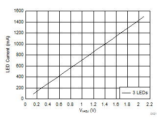
| VIN = 14 V |
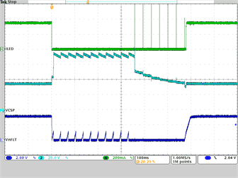
Ch2: CSP pin voltage;
Ch4: LED current; Time: 100 ms/div
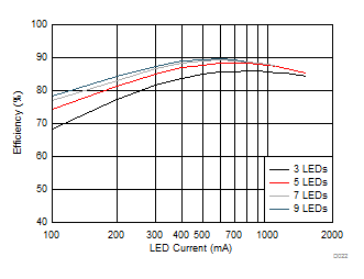
| VIN = 14 V |
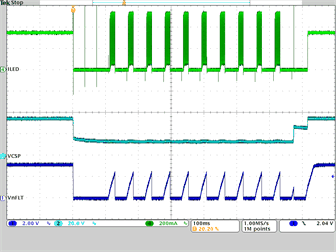
Ch2: CSP pin voltage;
Ch4: LED current; Time: 100 ms/div