SLVSDD9 March 2017 TPS92692 , TPS92692-Q1
PRODUCTION DATA.
- 1 Features
- 2 Applications
- 3 Description
- 4 Revision History
- 5 Pin Configuration and Functions
- 6 Specifications
-
7 Detailed Description
- 7.1 Overview
- 7.2 Functional Block Diagram
- 7.3
Feature Description
- 7.3.1 Internal Regulator and Undervoltage Lockout (UVLO)
- 7.3.2 Oscillator
- 7.3.3 Spread Spectrum Frequency Modulation
- 7.3.4 Gate Driver
- 7.3.5 Rail-to-Rail Current Sense Amplifier
- 7.3.6 Transconductance Error Amplifier
- 7.3.7 Switch Current Sense
- 7.3.8 Slope Compensation
- 7.3.9 Analog Adjust Input
- 7.3.10 DIM/PWM Input
- 7.3.11 Series P-Channel FET Dimming Gate Driver Output
- 7.3.12 Soft-Start
- 7.3.13 Current Monitor Output
- 7.3.14 Output Overvoltage Protection
- 7.3.15 Output Short-circuit Protection
- 7.3.16 Thermal Protection
- 7.3.17 Fault Indicator (FLT)
- 7.4 Device Functional Modes
-
8 Application and Implementation
- 8.1
Application Information
- 8.1.1 Duty Cycle Considerations
- 8.1.2 Inductor Selection
- 8.1.3 Output Capacitor Selection
- 8.1.4 Input Capacitor Selection
- 8.1.5 Main Power MOSFET Selection
- 8.1.6 Rectifier Diode Selection
- 8.1.7 LED Current Programming
- 8.1.8 Switch Current Sense Resistor
- 8.1.9 Slope Compensation
- 8.1.10 Feedback Compensation
- 8.1.11 Soft-Start
- 8.1.12 Overvoltage and Undervoltage Protection
- 8.1.13 Analog to PWM Dimming Considerations
- 8.1.14 Direct PWM Dimming Considerations
- 8.1.15 Series P-Channel MOSFET Selection
- 8.2
Typical Applications
- 8.2.1
Typical Boost LED Driver
- 8.2.1.1 Design Requirements
- 8.2.1.2
Detailed Design Procedure
- 8.2.1.2.1 Calculating Duty Cycle
- 8.2.1.2.2 Setting Switching Frequency
- 8.2.1.2.3 Setting Dither Modulation Frequency
- 8.2.1.2.4 Inductor Selection
- 8.2.1.2.5 Output Capacitor Selection
- 8.2.1.2.6 Input Capacitor Selection
- 8.2.1.2.7 Main N-Channel MOSFET Selection
- 8.2.1.2.8 Rectifying Diode Selection
- 8.2.1.2.9 Programming LED Current
- 8.2.1.2.10 Setting Switch Current Limit
- 8.2.1.2.11 Programming Slope Compensation
- 8.2.1.2.12 Deriving Compensator Parameters
- 8.2.1.2.13 Setting Start-up Duration
- 8.2.1.2.14 Setting Overvoltage Protection Threshold
- 8.2.1.2.15 Analog-to-PWM Dimming Considerations
- 8.2.1.3 Application Curves
- 8.2.2
Typical Buck-Boost LED Driver
- 8.2.2.1 Design Requirements
- 8.2.2.2
Detailed Design Procedure
- 8.2.2.2.1 Calculating Duty Cycle
- 8.2.2.2.2 Setting Switching Frequency
- 8.2.2.2.3 Setting Dither Modulation Frequency
- 8.2.2.2.4 Inductor Selection
- 8.2.2.2.5 Output Capacitor Selection
- 8.2.2.2.6 Input Capacitor Selection
- 8.2.2.2.7 Main N-Channel MOSFET Selection
- 8.2.2.2.8 Rectifier Diode Selection
- 8.2.2.2.9 Programming LED Current
- 8.2.2.2.10 Setting Switch Current Limit and Slope Compensation
- 8.2.2.2.11 Programming Slope Compensation
- 8.2.2.2.12 Deriving Compensator Parameters
- 8.2.2.2.13 Setting Startup Duration
- 8.2.2.2.14 Setting Overvoltage Protection Threshold
- 8.2.2.2.15 Direct PWM Dimming Consideration
- 8.2.2.3 Application Curves
- 8.2.1
Typical Boost LED Driver
- 8.1
Application Information
- 9 Power Supply Recommendations
- 10Layout
- 11Device and Documentation Support
- 12Mechanical, Packaging, and Orderable Information
Package Options
Mechanical Data (Package|Pins)
- PWP|20
Thermal pad, mechanical data (Package|Pins)
- PWP|20
Orderable Information
6 Specifications
6.1 Absolute Maximum Ratings
over operating free-air temperature range (unless otherwise noted)(1)(2)| MIN | MAX | UNIT | ||
|---|---|---|---|---|
| Input voltage | VIN, CSP, CSN | –0.3 | 65 | V |
| DIM/PWM | –0.3 | 14 | V | |
| IS, RT, FLT | –0.3 | 8.8 | V | |
| OV, SS, RAMP, DM, SLOPE, VREF, IADJ | –0.3 | 5.5 | V | |
| CSP to CSN(3) | –0.3 | 0.3 | V | |
| Output voltage(4) | VCC, GATE | –0.3 | 8.8 | V |
| PDRV | VCSP – 8.8 | VCSP | V | |
| COMP | –0.3 | 5.0 | V | |
| Source current | IMON | — | 100 | µA |
| GATE (pulsed < 20 ns) | — | 500 | mA | |
| PDRV (pulsed < 10 µs) | — | 50 | mA | |
| Sink current | GATE (pulsed < 20 ns) | — | 500 | mA |
| PDRV (pulsed < 10 µs) | — | 50 | mA | |
| Operating junction temperature, TJ | –40 | 150 | °C | |
| Storage temperature, Tstg | 165 | °C | ||
(1) Stresses beyond those listed under Absolute Maximum Ratings may cause permanent damage to the device. These are stress ratings only, which do not imply functional operation of the device at these or any other conditions beyond those indicated under Recommended Operating Conditions. Exposure to absolute-maximum-rated conditions for extended periods may affect device reliability.
(2) All voltages are with respect to GND unless otherwise noted
(3) Continuous sustaining voltage
(4) All output pins are not specified to have an external voltage applied.
6.2 ESD Ratings
| VALUE | UNIT | ||||
|---|---|---|---|---|---|
| TPS92692-Q1 IN PWP (HTSSOP) PACKAGE | |||||
| V(ESD) | Electrostatic discharge | Human-body model (HBM), per AEC Q100-002, all pins(1) | ±2000 | V | |
| Charged-device model (CDM), per AEC Q100-011 | All pins except 1, 10, 11, and 20 | ±500 | |||
| Pins 1, 10, 11, and 20 | ±750 | ||||
| TPS92692 IN PWP (HTSSOP) PACKAGE | |||||
| V(ESD) | Electrostatic discharge | Human-body model (HBM), per ANSI/ESDA/JEDEC JS-001, all pins(2) | ±2000 | V | |
| Charged-device model (CDM), per JEDEC specification JESD22-C101, all pins(3) | ±500 | ||||
(1) AEC Q100-002 indicates that HBM stressing shall be in accordance with the ANSI/ESDA/JEDEC JS-001 specification.
(2) JEDEC document JEP155 states that 500-V HBM allows safe manufacturing with a standard ESD control process.
(3) JEDEC document JEP157 states that 250-V CDM allows safe manufacturing with a standard ESD control process.
6.3 Recommended Operating Conditions
over operating free-air temperature range (unless otherwise noted)| MIN | NOM | MAX | UNIT | ||
|---|---|---|---|---|---|
| VIN | Supply input voltage | 6.5 | 14 | 65 | V |
| VIN, crank | Supply input, battery crank voltage | 4.5 | V | ||
| VCSP, VCSN | Current sense common mode | 6.5 | 60 | V | |
| ƒSW | Switching frequency | 80 | 800 | kHz | |
| ƒm | Spread spectrum modulation frequency | 0.1 | 12 | kHz | |
| fRAMP | Internal PWM ramp generator frequency | 100 | 2000 | Hz | |
| VIADJ | Current reference voltage | 0.14 | VIADJ(CLAMP) | V | |
| TA | Operating ambient temperature | –40 | 125 | °C | |
6.4 Thermal Information
| THERMAL METRIC(1) | TPS92692 | TPS92692-Q1 | UNIT | |
|---|---|---|---|---|
| PWP (HTSSOP) | PWP (HTSSOP) | |||
| 20 PINS | 20 PINS | |||
| RθJA | Junction-to-ambient thermal resistance | 40.8 | 40.8 | °C/W |
| RθJC(top) | Junction-to-case (top) thermal resistance | 26.1 | 26.1 | °C/W |
| RθJB | Junction-to-board thermal resistance | 22.2 | 22.2 | °C/W |
| ψJT | Junction-to-top characterization parameter | 0.8 | 0.8 | °C/W |
| ψJB | Junction-to-board characterization parameter | 22.0 | 22.0 | °C/W |
| RθJC(bot) | Junction-to-case (bottom) thermal resistance | 2.3 | 2.3 | °C/W |
(1) For more information about traditional and new thermal metrics, see the Semiconductor and IC Package Thermal Metrics application report.
6.5 Electrical Characteristics
–40°C ≤ TJ ≤ 150°C, VIN = 14 V, VIADJ = 2.1 V, VRAMP = 500 mV, VDIM/PWM = 3 V, VOV = 500 mV, CVCC = 1 µF, CVREF = 1 µF, CCOMP = 2.2 nF, RCS = 100 mΩ, RT = 20 kΩ, no load on GATE and PDRV (unless otherwise noted)(1)| PARAMETER | TEST CONDITIONS | MIN | TYP | MAX | UNIT | |
|---|---|---|---|---|---|---|
| INPUT VOLTAGE (VIN) | ||||||
| IIN(STBY) | Input stand-by current | VPWM = 0 V | 1.8 | 2.5 | mA | |
| IIN(SW) | Input switching current | VCC = 7.5 V, CGATE = 1 nF | 5.1 | 6.6 | mA | |
| BIAS SUPPLY (VCC) | ||||||
| VCC(REG) | Regulation voltage | No load | 7.0 | 7.5 | 8.0 | V |
| VCC(UVLO) | Supply undervoltage protection | VCC rising threshold, VIN = 8 V | 4.5 | 4.9 | V | |
| VCC falling threshold, VIN = 8 V | 3.7 | 4.1 | V | |||
| Hysteresis | 400 | mV | ||||
| ICC(LIMIT) | Supply current limit | VCC = 0 V | 30 | 36 | 46 | mA |
| VDO | LDO dropout voltage | ICC = 20 mA, VIN = 5 V | 300 | mV | ||
| REFERENCE VOLTAGE (VREF) | ||||||
| VREF | Reference voltage | No load | 4.77 | 4.96 | 5.15 | V |
| IREF(LIMIT) | Current limit | VREF = 0 V | 30 | 36 | 46 | mA |
| OSCILLATOR (RT) | ||||||
| ƒSW | Switching frequency | RT = 40 kΩ | 175 | 200 | 225 | kHz |
| RT = 20 kΩ | 341 | 390 | 439 | kHz | ||
| VRT | RT output voltage | 1 | V | |||
| VSYNC | SYNC rising threshold | VRT rising | 2.5 | 3.1 | V | |
| SYNC falling threshold | VRT falling | 1.8 | 2 | V | ||
| tSYNC(MIN) | Minimum SYNC clock pulse width | 100 | ns | |||
| SPREAD SPECTRUM FREQUENCY MODULATION (DM) | ||||||
| IDM | Triangle wave generator sink current | 10 | µA | |||
| Triangle wave generator source current | 10 | µA | ||||
| VDM(TR) | Triangle wave voltage peak (High) | 1.15 | V | |||
| Triangle wave voltage valley (Low) | 850 | mV | ||||
| VDM(EN) | Spread spectrum modulation enable threshold | 700 | mV | |||
| VDM(CLAMP) | Internal clamp voltage | VPWM = 0 V, RRAMP = 200 kΩ | 1.25 | V | ||
| GATE DRIVER (GATE) | ||||||
| RGH | Gate driver high side resistance | IGATE = –10 mA | 5.4 | 11.2 | Ω | |
| RGL | Gate driver low side resistance | IGATE = 10 mA | 4.3 | 10.5 | Ω | |
| CURRENT SENSE (IS) | ||||||
| VIS(LIMIT) | Current limit threshold | VDIM/PWM = 5 V, RRAMP = 249 kΩ | 230.6 | 250 | 270 | mV |
| VDIM/PWM = 0 V, RRAMP = 249 kΩ | 665 | 700 | 735 | mV | ||
| tIS(BLANK) | Leading edge blanking time | 88 | 118 | 158 | ns | |
| tIS(FAULT) | Current limit fault time | 35 | µs | |||
| tILMT(DLY) | IS to GATE propagation delay | VIS pulsed from 0 V to 1 V | 78 | ns | ||
| PWM COMPARATOR AND SLOPE COMPENSATION (SLOPE) | ||||||
| DMAX | Maximum duty cycle | 90 | % | |||
| VSLOPE | Adaptive slope compensation | VCSP = 24 V | 410 | mV | ||
| VSLOPE(MIN) | Minimum slope compensation output voltage | VCSP = 0 V | 72 | mV | ||
| VLV | IS to COMP level shift voltage | No slope compensation added | 1.42 | 1.60 | 1.82 | V |
| ILV | IS level shift bias current | No slope compensation added | 17 | µA | ||
| CURRENT SENSE AMPLIFIER (CSP, CSN) | ||||||
| V(CSP-CSN) | Current sense thresholds | VCSP = 14 V, VIADJ = 3 V | 163.4 | 170.7 | 177.6 | mV |
| VCSP = 14 V, VIADJ = 1.4 V | 95.83 | 100.5 | 103.85 | mV | ||
| CS(BW) | Current sense unity gain bandwidth | 500 | kHz | |||
| GCS | Current sense amplifier gain | G = VIADJ/V(CSP-CSN) | 14 | |||
| K(OCP) | Ratio of over-current detection threshold to analog adjust voltage | K (OCP) = V(OCP-THR)/VIADJ | 1.46 | 1.5 | 1.61 | |
| ICSP(BIAS) | CSP bias current | VCSN = 14.1 V, VCSP = 14 V | 107 | µA | ||
| ICSN(BIAS) | CSN bias current | VCSN = 14.1 V, VCSP = 14 V | 110 | µA | ||
| FAULT INDICATOR (FLT) | ||||||
| R(FLT) | Open-drain pull down resistance | 241 | Ω | |||
| t(FAULT_TMR) | Fault timer | 24 | 36 | 48 | ms | |
| CURRENT MONITOR (IMON) | ||||||
| IIMON(SRC) | IMON source current | V(CSP-CSN) = 150 mV, VIMON = 0 V |
144 | µA | ||
| VIMON(CLP) | IMON output voltage clamp | 3.2 | 3.7 | 4.2 | V | |
| VIMON(OS) | IMON buffer offset voltage | –7.2 | 0 | 8.5 | mV | |
| ANALOG ADJUST (IADJ) | ||||||
| VIADJ(CLP) | IADJ internal clamp voltage | IIADJ = 1 µA | 2.29 | 2.40 | 2.55 | V |
| IIADJ(BIAS) | IADJ input bias current | VIADJ < 2.2 V | 10.5 | nA | ||
| RIADJ(LMT) | IADJ current limiting series resistor | VIADJ > 2.6 V | 12 | kΩ | ||
| ERROR AMPLIFIER (COMP) | ||||||
| gM | Transconductance | 121 | µA/V | |||
| ICOMP(SRC) | COMP current source capacity | VIADJ = 1.4 V, V(CSP-CSN) = 0 V | 130 | µA | ||
| ICOMP(SINK) | COMP current sink capacity | VIADJ = 0 V, V(CSP-CSN) = 0.1 V | 130 | µA | ||
| EA(BW) | Error amplifier bandwidth | Gain = –3 dB | 5 | MHz | ||
| VCOMP(RST) | COMP pin reset voltage | 100 | mV | |||
| RCOMP(DCH) | COMP discharge FET resistance | 246 | Ω | |||
| SOFT-START (SS) | ||||||
| ISS | Soft-start source current | 7 | 10 | 12.8 | µA | |
| VSS(UVP_EN) | Soft-start voltage threshold to enable output under-voltage protection | 2.4 | V | |||
| VSS(RST) | Soft-start pin reset voltage | 50 | mV | |||
| RSS(DCH) | SS discharge FET resistance | 240 | Ω | |||
| OUTPUT VOLTAGE INPUT (OV) | ||||||
| VOVP(THR) | Overvoltage protection threshold | 1.195 | 1.228 | 1.262 | V | |
| VUVP(THR) | Undervoltage protection threshold | 81.7 | 100 | 115.1 | mV | |
| t(UVP-BLANK) | Undervoltage protection blanking period | 4 | µs | |||
| IOVP(HYS) | OVP hysteresis current | 12 | 20 | 27.5 | µA | |
| INTERNAL PWM RAMP GENERATOR (RAMP) | ||||||
| IRAMP | Ramp generator source current | 7.75 | 10 | 12.73 | µA | |
| Ramp generator sink current | 8.24 | 10 | 12.41 | µA | ||
| VRAMP | Ramp signal peak (high) | 3 | V | |||
| Ramp signal valley (low) | 1 | V | ||||
| PWM INPUT (DIM/PWM) | ||||||
| VPWM(HIGH) | Schmitt trigger logic level (high threshold) | VRAMP = 2.0 V | 2.0 | 2.2 | V | |
| VPWM(LOW) | Schmitt trigger logic level (low threshold) | VRAMP = 2.0 V | 1.8 | 2.0 | V | |
| RPWM(PD) | PWM pull-down resistance | 10 | MΩ | |||
| tDLY(RISE) | PWM rising to PDRV delay | CPDRV = 1 nF | 294 | ns | ||
| tDLY(FALL) | PWM falling to PDRV delay | CPDRV = 1 nF | 326 | ns | ||
| SERIES P-CHANNEL PWM FET GATE DRIVE OUTPUT (PDRV) | ||||||
| VPDRV(OFF) | P-channel gate driver off-state voltage | VCSP = 14 V | 14 | V | ||
| VPDRV(ON) | P-channel gate driver on-state voltage | VCSP = 14 V | 7.4 | V | ||
| IPDRV(SRC) | PDRV sink current | Pulsed | 50 | mA | ||
| RPDRV(L) | PDRV driver pull up resistance | 82 | Ω | |||
| THERMAL SHUTDOWN | ||||||
| TSD | Thermal shutdown temperature | 175 | °C | |||
| TSD(HYS) | Thermal shutdown hysteresis | 25 | °C | |||
(1) All voltages are with respect to GND unless otherwise noted
6.6 Typical Characteristics
TA = 25°C, VIN = 14 V, VIADJ = 2.2 V, CVCC = 1 µF, CCOMP = 2.2 nF, RCS = 100 mΩ, RT = 20 kΩ, VPWM = 5 V, no load on GATE and PDRV (unless otherwise noted)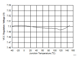 Figure 1. VCC Regulation Voltage vs Junction Temperature
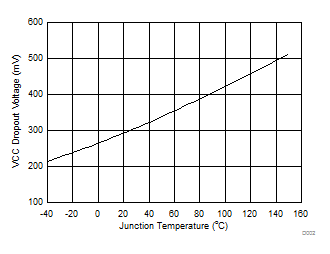
| VIN = 5 V, | IVCC= 20 mA |
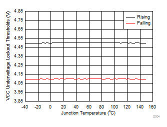 Figure 5. VCC UVLO Threshold vs Junction Temperature
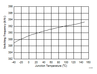
| RT= 20 kΩ |
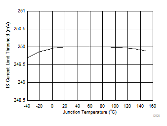 Figure 9. Current Limit Threshold vs Junction Temperature
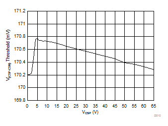
| VIADJ> 2.6 V |
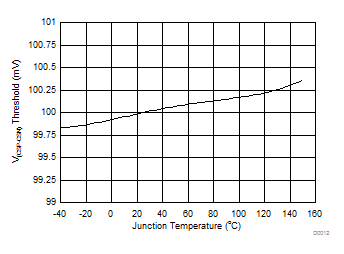
| VIADJ= 1.4 V |
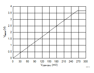 Figure 15. VIMON vs V(CSP-CSN)
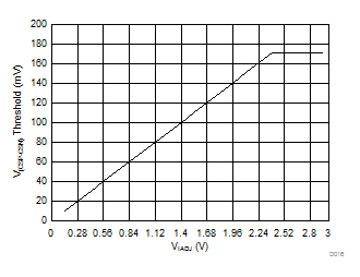 Figure 17. V(CSP-CSN) Threshold vs VIADJ
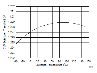 Figure 19. OVP Detection Threshold vs Junction Temperature
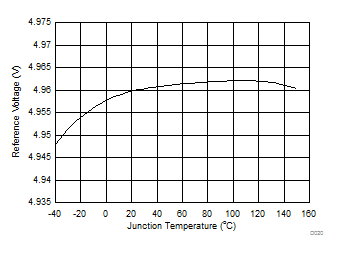 Figure 2. VREF Reference Voltage vs Junction Temperature
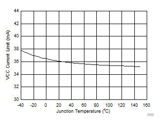 Figure 4. VCC Current Limit vs Junction Temperature
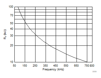 Figure 6. Timing Resistance (RT) vs Switching Frequency
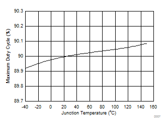 Figure 8. Maximum Duty Cycle vs Junction Temperature
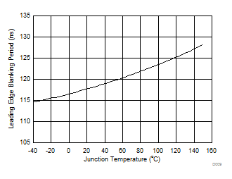 Figure 10. Leading Edge Blanking Period vs Junction Temperature
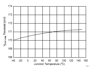
| VIADJ> 2.6 V |
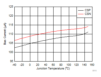
| VCSP= VCSN = 14 V |
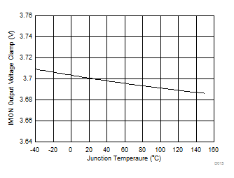 Figure 16. VIMON(CLP) vs Junction Temperature
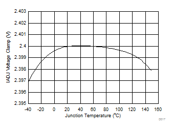 Figure 18. VIADJ Voltage Clamp vs Junction Temperature
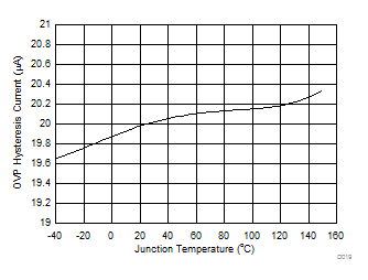 Figure 20. OVP Hysteresis Current vs Junction Temperature