SLVSFZ4A December   2020  – February 2021 TPS929121-Q1

PRODUCTION DATA  

  1. Features
  2. Applications
  3. Description
  4. Revision History
  5. Device Comparison Table
  6. Pin Configuration and Functions
  7. Specifications
    1. 7.1 Absolute Maximum Ratings
    2. 7.2 ESD Ratings
    3. 7.3 Recommended Operating Conditions
    4. 7.4 Thermal Information
    5. 7.5 Electrical Characteristics
    6. 7.6 Timing Requirements
    7. 7.7 Typical Characteristics
  8. Detailed Description
    1. 8.1 Overview
    2. 8.2 Functional Block Diagram
    3. 8.3 Feature Description
      1. 8.3.1 Device Bias and Power
        1. 8.3.1.1 Power Supply (SUPPLY)
        2. 8.3.1.2 5-V Low-Drop-Out Linear Regulator (VLDO)
        3. 8.3.1.3 Undervoltage Lockout (UVLO) and Power-On-Reset (POR)
        4. 8.3.1.4 Programmable Low Supply Warning
      2. 8.3.2 Constant Current Output
        1. 8.3.2.1 Reference Current With External Resistor (REF)
        2. 8.3.2.2 64-Step Programmable High-Side Constant-Current Output
      3. 8.3.3 PWM Dimming
        1. 8.3.3.1 PWM Dimming Frequency
        2. 8.3.3.2 PWM Generator
        3. 8.3.3.3 Linear Brightness Control
        4. 8.3.3.4 Exponential Brightness Control
        5. 8.3.3.5 External Clock Input for PWM Generator (CLK)
        6. 8.3.3.6 External PWM Input ( PWM0 and PWM1)
      4. 8.3.4 On-chip 8-bit Analog-to-Digital Converter (ADC)
      5. 8.3.5 Diagnostic and Protection in Normal State
        1. 8.3.5.1  Fault Masking
        2. 8.3.5.2  Supply Undervoltage Lockout Diagnostics in Normal State
        3. 8.3.5.3  Low-Supply Warning Diagnostics in Normal State
        4. 8.3.5.4  Reference Diagnostics in Normal State
        5. 8.3.5.5  Pre-Thermal Warning and Overtemperature Protection in Normal State
        6. 8.3.5.6  Communication Loss Diagnostic in Normal State
        7. 8.3.5.7  LED Open-Circuit Diagnostics in Normal State
        8. 8.3.5.8  LED Short-Circuit Diagnostics in Normal State
        9. 8.3.5.9  On-Demand Off-State Invisible Diagnostics
        10. 8.3.5.10 On-Demand Off-State Single-LED Short-Circuit (SS) Diagnostics
        11. 8.3.5.11 Automatic Single-LED Short-Circuit (AutoSS) Detection in Normal State
        12. 8.3.5.12 EEPROM CRC Error in Normal State
        13.       48
      6. 8.3.6 Diagnostic and Protection in Fail-Safe States
        1. 8.3.6.1 Fault Masking
        2. 8.3.6.2 Supply UVLO Diagnostics in Fail-Safe States
        3. 8.3.6.3 Low-supply Warning Diagnostics in Fail-Safe states
        4. 8.3.6.4 Reference Diagnostics at Fail-Safe States
        5. 8.3.6.5 Overtemperature Protection in Fail-Safe State
        6. 8.3.6.6 LED Open-circuit Diagnostics in Fail-Safe State
        7. 8.3.6.7 LED Short-circuit Diagnostics in Fail-Safe State
        8. 8.3.6.8 EEPROM CRC Error in Fail-safe State
        9.       58
    4. 8.4 Device Functional Modes
      1. 8.4.1 POR State
      2. 8.4.2 Initialization State
      3. 8.4.3 Normal State
      4. 8.4.4 Fail-Safe States
      5. 8.4.5 Program State
      6. 8.4.6 Programmable Output Failure State
      7. 8.4.7 ERR Output
      8. 8.4.8 Register Default Data
    5. 8.5 Programming
      1. 8.5.1 FlexWire Protocol
        1. 8.5.1.1 Protocol Overview
        2. 8.5.1.2 UART Interface Address Setting
        3. 8.5.1.3 Status Response
        4. 8.5.1.4 Synchronization Byte
        5. 8.5.1.5 Device Address Byte
        6. 8.5.1.6 Register Address Byte
        7. 8.5.1.7 Data Frame
        8.       77
        9. 8.5.1.8 CRC Frame
        10. 8.5.1.9 Burst Mode
      2. 8.5.2 Registers Lock
      3. 8.5.3 All Registers CRC Check
      4. 8.5.4 EEPROM Programming
        1. 8.5.4.1 Chip Selection by Pulling REF Pin High
        2. 8.5.4.2 Chip Selection by ADDR Pins configuration
        3. 8.5.4.3 EEPROM Register Access and Burn
        4. 8.5.4.4 EEPROM Program State Exit
        5. 8.5.4.5 Reading Back EEPROM
    6. 8.6 Register Maps
      1. 8.6.1 FullMap Registers
  9. Application and Implementation
    1. 9.1 Application Information
    2. 9.2 Typical Application
      1. 9.2.1 Smart Rear Lamp With Distributed LED drivers
      2. 9.2.2 Design Requirements
      3. 9.2.3 Detailed Design Procedure
      4. 9.2.4 Application Curves
  10. 10Power Supply Recommendations
  11. 11Layout
    1. 11.1 Layout Guidelines
    2. 11.2 Layout Example
  12. 12Device and Documentation Support
    1. 12.1 Receiving Notification of Documentation Updates
    2. 12.2 Support Resources
    3. 12.3 Trademarks
    4. 12.4 Electrostatic Discharge Caution
    5. 12.5 Glossary
  13. 13Mechanical, Packaging, and Orderable Information

Package Options

Mechanical Data (Package|Pins)
Thermal pad, mechanical data (Package|Pins)
Orderable Information

Typical Characteristics

GUID-8550F862-7CAB-4FD5-AB84-39C83C02D6E1-low.gif
R(REF) = 8.35 kΩ
CONF_REFRANGE[1:0] = 3h
Figure 7-1 Fault Current vs Supply Voltage
GUID-4D89F4AF-27C2-4A4D-88DE-D08764F18221-low.gif
CONF_IOUTx[5:0] = 3Fh
CONF_REFRANGE[1:0] = 3h
Figure 7-3 Output Full-range Current vs REF Resistor
GUID-87ECE1AF-F3D4-4323-824F-CF303A3CC2E9-low.gif
R(REF) = 12.6 kΩ
CONF_IOUTx[5:0] = 3Fh
Figure 7-5 Output Current vs Dropout Voltage
GUID-1B52DD87-A9ED-4298-B0B1-BB7F5CE62751-low.gif
R(REF) = 12.6 kΩ
CONF_IOUTx[5:0] = 3Fh
Figure 7-7 Average Current vs PWMOUT[7:0]
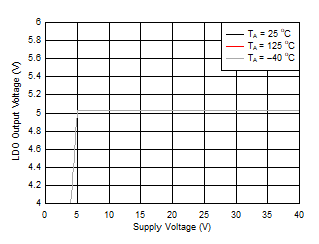
GUID-C5C7162C-52BE-429C-B45C-76DCDBB815E8-low.gifFigure 7-9 LDO Output Line Regulation
GUID-BF16EE5E-9FD7-456C-B085-2F0492775CC4-low.gif
CONF_REFRANGE[1:0] = 3h
Figure 7-2 Standby Current vs REF Resistor
GUID-0FE73D0E-D936-4371-9551-75B0B8052051-low.gif
CONF_REFRANGE[1:0] = 3h
Figure 7-4 Output Current vs Dropout Voltage
GUID-04E13A8C-3631-437A-B55D-50250F085BA2-low.gif
CONF_REFRANGE[1:0] = 3h
Figure 7-6 Output Current vs Supply Voltage
GUID-7EF7CCFD-C07F-40B2-89EF-4D44393CF08C-low.gif
R(REF) = 8.35 kΩ & 12.6 kΩ
CONF_REFRANGE[1:0] = 3h
Figure 7-8 Output DC Current vs IOUT[5:0]
GUID-C9721F56-FE66-496F-BB5C-6E5C5876821C-low.gifFigure 7-10 LDO Output Load Regulation
GUID-D775298E-7DEE-48E3-B6B8-95749F4521AE-low.gif
Ch1 = V(SUPPLY)Ch3 = V(OUT0)Ch6 = I(OUT0)
Figure 7-11 PWM Dimming at 200 Hz
GUID-6FE7E61A-6BBF-4A24-B537-A82D54F58EBE-low.gif
Ch1 = V(SUPPLY)Ch3 = V(OUT0)Ch6 = I(OUT0)
Figure 7-13 Supply Dimming In Fail-Safe Mode
GUID-73AC8CF2-4AE9-4CA5-A4F3-7C2AB9675C19-low.gif
Ch1 = V(SUPPLY)Ch2 = ERRCh3 = V(OUT0)
Ch6 = I(OUT0)
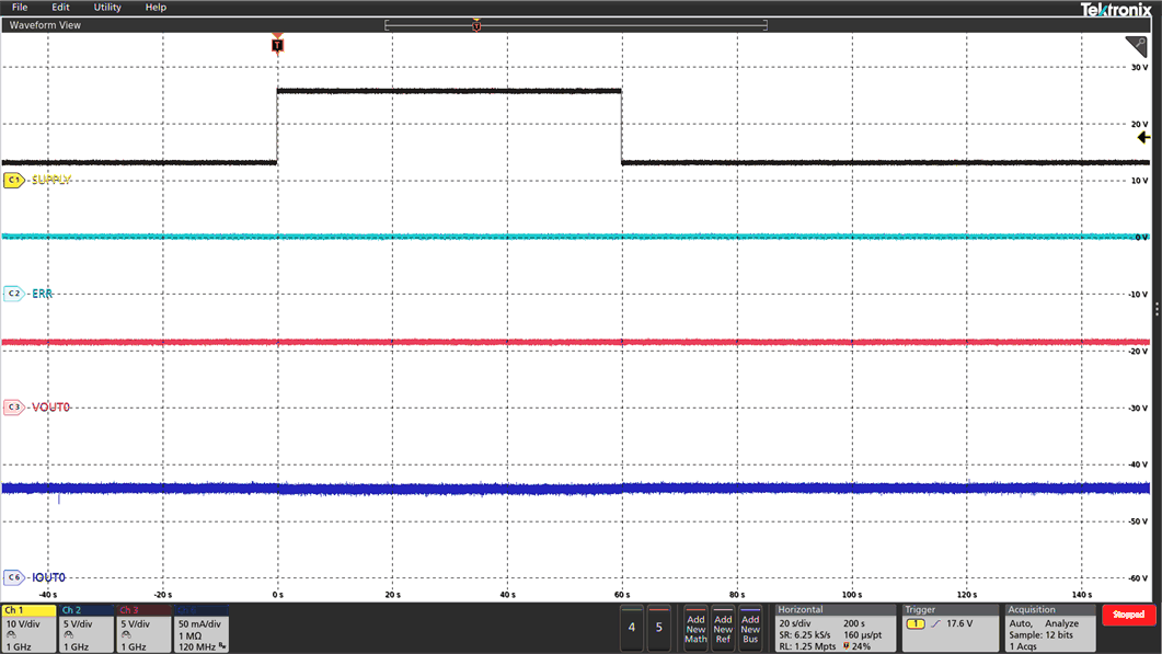
Figure 7-15 Transient Overvoltage
GUID-ADAD5F1B-B71D-48F5-8BEB-68F0CD36784B-low.gif
Ch1 = V(SUPPLY)Ch2 = ERRCh3 = V(OUT0)
Ch6 = I(OUT0)
Figure 7-17 Superimposed Alternating Voltage 15 Hz
GUID-B25BCB50-14F6-4EB6-9278-C3FA4E533C86-low.gif
Ch1 = V(SUPPLY)Ch2 = ERRCh3 = V(OUT0)
Ch4 = V(LDO)Ch6 = I(OUT0)
Figure 7-19 Slow Decrease and Quick Increase of Supply Voltage
GUID-F2729AF4-7064-4C0A-83A9-B97EBBC369AF-low.gif
Ch1 = V(SUPPLY)Ch2 = ERRCh4 = V(LDO)
Ch6 = I(LDO)0 to 80 mA
Figure 7-21 LDO Output Load Transient
GUID-75E22150-7272-45F3-98EB-1E0919696369-low.gif
Ch1 = V(SUPPLY)Ch2 = ERRCh3 = V(OUT0)
Ch6 = I(OUT0)T(ODPW) = 100 µsF(PWM) = 2 kHz
Figure 7-23 LED Short-Circuit Detection In Normal Mode
GUID-556B3747-6507-41FF-865F-975EC73431F6-low.gif
Ch1 = V(SUPPLY)Ch2 = ERRCh3 = V(OUT5)
Ch6 = I(OUT0)T(ODPW) = 100 µsF(PWM) = 2 kHz
Figure 7-25 LED Open-Circuit Detection In FS Mode
GUID-D9F43757-310C-4895-9AAE-6AFDE7CA17E2-low.gif
Ch1 = V(SUPPLY)Ch2 = ERRCh3 = V(OUT5)
Ch6 = I(OUT0)T(ODPW) = 100 µsF(PWM) = 2 kHz
Figure 7-27 LED Short-Circuit Detection In Fail-Safe Mode
GUID-3D0E2507-4592-4AD4-8782-A5069DD97C9D-low.gif
Ch1 = V(SUPPLY)Ch3 = V(OUT0)Ch6 = I(OUT0)
Figure 7-12 PWM Dimming at 2000 Hz
GUID-3B6B0175-6ECD-4E80-8D71-E0C839A5E022-low.gif
Ch1 = V(SUPPLY)Ch2 = ERRCh3 = V(OUT0)
Ch6 = I(OUT0)
Figure 7-14 Transient Undervoltage
GUID-A4F96D8F-1614-4EEF-B78F-880E58B883DB-low.gif
Ch1 = V(SUPPLY)Ch2 = ERRCh3 = V(OUT0)
Ch6 = I(OUT0)
Figure 7-16 Jump Start
GUID-1BC57D55-DDD7-43B8-B812-8551D837E912-low.gif
Ch1 = V(SUPPLY)Ch2 = ERRCh3 = V(OUT0)
Ch6 = I(OUT0)
Figure 7-18 Superimposed Alternating Voltage 1 kHz
GUID-6CDE13AF-7705-4F47-88FC-6283D0179E2F-low.gif
Ch1 = V(SUPPLY)Ch2 = ERRCh3 = V(OUT0)
Ch4 = V(LDO)Ch6 = I(OUT0)
Figure 7-20 Slow Decrease and Slow Increase of Supply Voltage
GUID-81332EE4-E8FF-4FBD-81AA-65952118A164-low.gif
Ch1 = V(SUPPLY)Ch2 = ERRCh3 = V(OUT0)
Ch6 = I(OUT0)T(ODPW) = 100 µsF(PWM) = 2 kHz
Figure 7-22 LED Open-Circuit Detection In Normal Mode
GUID-5772E6DE-1642-46E3-B997-1AF96A97196F-low.gif
Ch1 = V(SUPPLY)Ch2 = ERRCh3 = V(OUT5)
Ch6 = I(OUT5)T(ODPW) = 100 µsF(PWM) = 2 kHz
V(ADCSHORTTH) = 4 V
Figure 7-24 Single-LED Short-Circuit Detection In Normal Mode
GUID-DEBF0286-B1B3-4712-A80F-67EDA0EE02F3-low.gif
Ch1 = V(SUPPLY)Ch2 = ERRCh3 = V(OUT5)
Ch6 = I(OUT0)T(ODPW) = 100 µsF(PWM) = 2 kHz
Figure 7-26 LED Open-Circuit Recovery In FS Mode
GUID-F3AEF0B2-5E7F-4422-BF80-BE806D87636F-low.gif
Ch1 = V(SUPPLY)Ch2 = ERRCh3 = V(OUT5)
Ch6 = I(OUT0)T(ODPW) = 100 µsF(PWM) = 2 kHz
Figure 7-28 LED Short-Circuit Recovery In Fail-Safe Mode