SLVSFU7B July 2022 – April 2024 TPS929240-Q1
PRODUCTION DATA
- 1
- 1 Features
- 2 Applications
- 3 Description
- 4 Pin Configuration and Functions
- 5 Specifications
-
6 Detailed Description
- 6.1 Overview
- 6.2 Functional Block Diagram
- 6.3
Feature Description
- 6.3.1 Device Bias and Power
- 6.3.2 Constant Current Output
- 6.3.3 PWM Dimming
- 6.3.4 FAIL-SAFE State Operation
- 6.3.5 On-Chip, 8-Bit, Analog-to-Digital Converter (ADC)
- 6.3.6
Diagnostic and Protection in NORMAL State
- 6.3.6.1 VBAT Undervoltage Lockout Diagnostics in NORMAL state
- 6.3.6.2 Low-Supply Warning Diagnostics in NORMAL State
- 6.3.6.3 Supply Undervoltage Diagnostics in NORMAL State
- 6.3.6.4 Reference Diagnostics in NORMAL state
- 6.3.6.5 Pre-Thermal Warning in NORMAL state
- 6.3.6.6 Overtemperature Protection in NORMAL state
- 6.3.6.7 Overtemperature Shutdown in NORMAL state
- 6.3.6.8 LED Open-Circuit Diagnostics in NORMAL state
- 6.3.6.9 LED Short-Circuit Diagnostics in NORMAL state
- 6.3.6.10 Single-LED Short-Circuit Detection in NORMAL state
- 6.3.6.11 EEPROM CRC Error in NORMAL state
- 6.3.6.12 Communication Loss Diagnostic in NORMAL State
- 6.3.6.13 Fault Masking in NORMAL state
- 53
- 6.3.7
Diagnostic and Protection in FAIL-SAFE states
- 6.3.7.1 Supply Undervoltage Lockout Diagnostics in FAIL-SAFE states
- 6.3.7.2 Low-Supply Warning Diagnostics in FAIL-SAFE states
- 6.3.7.3 Supply Undervoltage Diagnostics in FAIL-SAFE State
- 6.3.7.4 Reference Diagnostics in FAIL-SAFE states
- 6.3.7.5 Pre-Thermal Warning in FAIL-SAFE state
- 6.3.7.6 Overtemperature Protection in FAIL-SAFE state
- 6.3.7.7 Overtemperature Shutdown in FAIL-SAFE state
- 6.3.7.8 LED Open-Circuit Diagnostics in FAIL-SAFE state
- 6.3.7.9 LED Short-Circuit Diagnostics in FAIL-SAFE state
- 6.3.7.10 Single-LED Short-Circuit Detection in FAIL-SAFE state
- 6.3.7.11 EEPROM CRC Error in FAIL-SAFE State
- 6.3.7.12 Fault Masking in FAIL-SAFE state
- Diagnostics Table in FAIL-SAFE State
- 6.3.8 OFAF Setup In FAIL-SAFE state
- 6.3.9 ERR Output
- 6.4 Device Functional Modes
- 6.5 Programming
- 6.6 Register Maps
- 7 Application and Implementation
- 8 Device and Documentation Support
- 9 Revision History
- 10Mechanical, Packaging, and Orderable Information
Package Options
Refer to the PDF data sheet for device specific package drawings
Mechanical Data (Package|Pins)
- DCP|38
Thermal pad, mechanical data (Package|Pins)
- DCP|38
Orderable Information
4 Pin Configuration and Functions
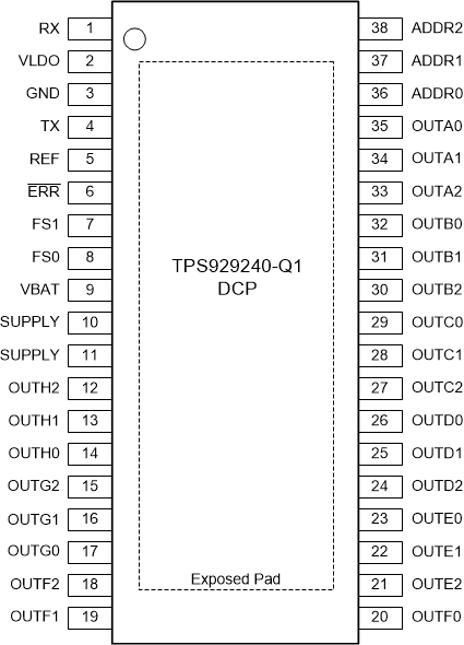
 Figure 4-1 DCP Package38-Pin HTSSOP with PowerPAD™ Integrated Circuit PackageTop View
Table 4-1 Pin Functions
| PIN | I/O | DESCRIPTION | |
|---|---|---|---|
| NO. | NAME | ||
| 1 | RX | I | FlexWire RX |
| 2 | VLDO | Power | 5V regulator output |
| 3 | GND | ̶ | Ground |
| 4 | TX | O | FlexWire TX |
| 5 | REF | I/O | Device current reference setting |
| 6 | ERR | I/O | Open-drain error indication |
| 7 | FS1 | I | Fail-safe input 1 |
| 8 | FS0 | I | Fail-safe input 0 |
| 9 | VBAT | Power | Power supply for analog and digital circuit |
| 10 | SUPPLY | Power | Power supply for current output channels |
| 11 | SUPPLY | Power | Power supply for current output channels |
| 12 | OUTH2 | O | Current output channel H2 |
| 13 | OUTH1 | O | Current output channel H1 |
| 14 | OUTH0 | O | Current output channel H0 |
| 15 | OUTG2 | O | Current output channel G2 |
| 16 | OUTG1 | O | Current output channel G1 |
| 17 | OUTG0 | O | Current output channel G0 |
| 18 | OUTF2 | O | Current output channel F2 |
| 19 | OUTF1 | O | Current output channel F1 |
| 20 | OUTF0 | O | Current output channel F0 |
| 21 | OUTE2 | O | Current output channel E2 |
| 22 | OUTE1 | O | Current output channel E1 |
| 23 | OUTE0 | O | Current output channel E0 |
| 24 | OUTD2 | O | Current output channel D2 |
| 25 | OUTD1 | O | Current output channel D1 |
| 26 | OUTD0 | O | Current output channel D0 |
| 27 | OUTC2 | O | Current output channel C2 |
| 28 | OUTC1 | O | Current output channel C1 |
| 29 | OUTC0 | O | Current output channel C0 |
| 30 | OUTB2 | O | Current output channel B2 |
| 31 | OUTB1 | O | Current output channel B1 |
| 32 | OUTB0 | O | Current output channel B0 |
| 33 | OUTA2 | O | Current output channel A2 |
| 34 | OUTA1 | O | Current output channel A1 |
| 35 | OUTA0 | O | Current output channel A0 |
| 36 | ADDR0 | I | Device address setting (Bit0) |
| 37 | ADDR1 | I | Device address setting (Bit1) |
| 38 | ADDR2 | I | Device address setting (Bit2) |