DLPS202A October 2020 – August 2024 TPS99000S-Q1
PRODUCTION DATA
- 1
- 1 Features
- 2 Applications
- 3 Description
- 4 Pin Configuration and Functions
-
5 Specifications
- 5.1 Absolute Maximum Ratings
- 5.2 ESD Ratings
- 5.3 Recommended Operating Conditions
- 5.4 Thermal Information
- 5.5 Electrical Characteristics—Transimpedance Amplifier Parameters
- 5.6 Electrical Characteristics—Digital to Analog Converters
- 5.7 Electrical Characteristics—Analog to Digital Converter
- 5.8 Electrical Characteristics—FET Gate Drivers
- 5.9 Electrical Characteristics—Photo Comparator
- 5.10 Electrical Characteristics—Voltage Regulators
- 5.11 Electrical Characteristics—Temperature and Voltage Monitors
- 5.12 Electrical Characteristics—Current Consumption
- 5.13 Power-Up Timing Requirements
- 5.14 Power-Down Timing Requirements
- 5.15 Timing Requirements—Sequencer Clock
- 5.16 Timing Requirements—Host and Diagnostic Port SPI Interface
- 5.17 Timing Requirements—ADC Interface
- 5.18 Switching Characteristics
-
6 Detailed Description
- 6.1 Overview
- 6.2 Functional Block Diagram
- 6.3
Feature Description
- 6.3.1
Illumination Control
- 6.3.1.1 Illumination System High Dynamic Range Dimming Overview
- 6.3.1.2 Illumination Control Loop
- 6.3.1.3 Continuous Mode Operation
- 6.3.1.4
Discontinuous Mode Operation
- 6.3.1.4.1 Discontinuous Mode Pulse Width Limit
- 6.3.1.4.2 COMPOUT_LOW Timer in Discontinuous Operation
- 6.3.1.4.3 Dimming Within Discontinuous Operation Range
- 6.3.1.4.4 Multiple Pulse Heights to Increase Bit Depth
- 6.3.1.4.5 TIA Gain Adjustment
- 6.3.1.4.6 Current Limit in Discontinuous Mode
- 6.3.1.4.7 CMODE Big Cap Mode in Discontinuous Operation
- 6.3.2 Over-Brightness Detection
- 6.3.3 Analog to Digital Converter
- 6.3.4 Power Sequencing and Monitoring
- 6.3.5 DMD Mirror Voltage Regulator
- 6.3.6 Low Dropout Regulators
- 6.3.7 System Monitoring Features
- 6.3.8 Communication Ports
- 6.3.1
Illumination Control
- 6.4 Device Functional Modes
- 6.5 Register Maps
- 7 Application and Implementation
- 8 Power Supply Recommendations
- 9 Layout
- 10Device and Documentation Support
- 11Revision History
- 12Mechanical, Packaging, and Orderable Information
Package Options
Mechanical Data (Package|Pins)
- PZP|100
Thermal pad, mechanical data (Package|Pins)
- PZP|100
Orderable Information
6.3.6 Low Dropout Regulators
The TPS99000S-Q1 includes four low drop out regulators, dedicated to specific internal functions:
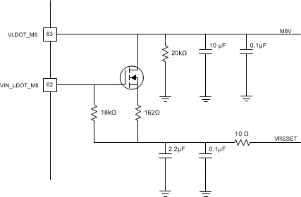
- A fixed –8V negative regulator for photodiode reverse biasing (VIN_LDOT_M8 input, VLDOT_M8 output)
- A 5V output regulator for internal analog circuits (VIN_LDOT_5V input, VLDOT_5V output)
- A 3.3V output regulator for internal analog (VIN_LDOT_3P3V input, VLDOT_3P3V output)
- A 3.3V output regulator dedicated to the ADC block (VIN_LDOA_3P3 input, VLDOA_3P3 output)
The positive output LDO regulators are all designed to operate from the same nominal 6V input as is needed by the LED selection FET gate driver supply input, DRVR_PWR, and the DMD mirror voltage regulator, VIN_DRST. However, care must be taken to isolate the sensitive analog circuit power supply inputs from switching noise, through dedicated sub-planes and supply filtering techniques. Noise on the analog supply rails will directly impact system dimming range performance, limiting stable operation at low brightness levels.
The negative 8V LDO is designed to use the DMD_VRESET power rail as its power source. (Note that this usage implies that the TIA/photodiode path will not be available for use until the DMD is in a powered-up state.)
 Figure 6-32 Negative 8V LDO Circuit
Applications that do not use a photodiode do not require the -8V regulator. VLDOT_M8 and VIN_LDOT_M8 may be left disconnected if the option in the DLPC230 SW to prevent enabling of the –8V LDO is selected. If these pins are not connected, care must be taken to confirm that the -8V LDO is not enabled. If this regulator is enabled while the pins are disconnected, permanent damage may be caused to the device.