-
TPSM265R1 65-V Input, 100-mA Power Module with Ultra-Low IQ
- 1 Features
- 2 Applications
- 3 Description
- 4 Revision History
- 5 Pin Configuration and Functions
-
6 Specifications
- 6.1 Absolute Maximum Ratings
- 6.2 ESD Ratings
- 6.3 Recommended Operating Conditions
- 6.4 Thermal Information
- 6.5 Electrical Characteristics
- 6.6 Typical Characteristics (VIN = 5 V)
- 6.7 Typical Characteristics (VIN = 12 V)
- 6.8 Typical Characteristics (VIN = 24 V)
- 6.9 Typical Characteristics (VIN = 48 V)
- 6.10 Typical Characteristics (VIN = 65 V)
-
7 Detailed Description
- 7.1 Overview
- 7.2 Functional Block Diagram
- 7.3
Feature Description
- 7.3.1 Adjustable Output Voltage (FB)
- 7.3.2 Input Capacitor Selection
- 7.3.3 Output Capacitor Selection
- 7.3.4 Precision Enable (EN), Undervoltage Lockout (UVLO), and Hysteresis (HYS)
- 7.3.5 PFM Operation
- 7.3.6 Power Good (PGOOD)
- 7.3.7 Configurable Soft Start (SS)
- 7.3.8 Overcurrent Protection (OCP)
- 7.3.9 Thermal Shutdown
- 7.4 Device Functional Modes
- 8 Applications and Implementation
- 9 Power Supply Recommendations
- 10Layout
- 11Device and Documentation Support
- 12Mechanical, Packaging, and Orderable Information
- IMPORTANT NOTICE
Package Options
Mechanical Data (Package|Pins)
- SIL|10
Thermal pad, mechanical data (Package|Pins)
Orderable Information
TPSM265R1 65-V Input, 100-mA Power Module with Ultra-Low IQ
1 Features
- Wide input voltage range of 3 V to 65 V
- Output voltage options:
- Adjustable 1.223 V to 15 V
- Fixed 3.3 V or 5 V
- 100-mA output current
- 10.5-µA quiescent current
- ±1% internal voltage reference
- PFM mode of operation
- –40°C to 125°C ambient temperature range
- Active slew rate control for low EMI
- Meets CISPR11 (EN55011) EMI standards
- Monotonic start-up into prebiased output
- Power-good flag
- Precision enable and input UVLO with hysteresis
- Thermal shutdown protection with hysteresis
- 2.8-mm x 3.7-mm x 1.9-mm package
- Create a custom regulator design with the TPSM265R1 using WEBENCH® Power Designer
3 Description
The TPSM265R1 is a compact, easy-to-use module that operates over a wide input voltage range up to a maximum continuous input voltage of 65 V. The module fully integrates a controller, MOSFETs, and an output inductor. The module is designed to quickly and easily implement a power design in a small PCB footprint. There are two fixed output voltage options, 3.3 V and 5 V, and an adjustable output voltage option that can be adjusted from 1.223 V to 15 V. Each option has a load current rating of 100 mA. The TPSM265R1 operates in Pulse Frequency Modulation (PFM) mode, providing optimal efficiency at light loads. The control scheme does not require loop compensation, providing excellent line and load transient.
Although designed for small size and simplicity, the TPSM265R1 offers many features. Precision enable, adjustable UVLO, and hysteresis allow for specific power-up and power-down requirements. Selectable/adjustable start-up timing options include minimum delay (no soft start), internally fixed (900 µs), and externally programmable soft start via an external capacitor. An open-drain PGOOD indicator can be used for sequencing and output voltage monitoring. The very small 2.8-mm × 3.7-mm × 1.9-mm package is a good fit for space-constrained applications.
| PART NUMBER(1) | OUTPUT | PACKAGE |
|---|---|---|
| TPSM265R1 | 1.223 V to 15 V | uSiP |
| TPSM265R1V3 | 3.3 V | |
| TPSM265R1V5 | 5 V |
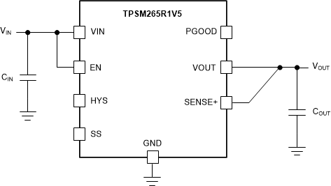
 Typical Schematic, Fixed Output
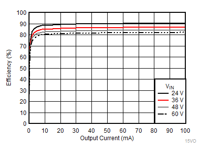
 Typical Efficiency, VOUT = 15
V
Typical Efficiency, VOUT = 15
V5 Pin Configuration and Functions
 Figure 5-1 10-Pin uSiP Exposed Thermal PadSIL-10C
Package(Top View)
Figure 5-1 10-Pin uSiP Exposed Thermal PadSIL-10C
Package(Top View)| PIN | TYPE(1) | DESCRIPTION | |
|---|---|---|---|
| NO. | NAME | ||
| 1 | VOUT | O | Output voltage pin. The VOUT pin is connected to the internal output inductor. Connect the VOUT pin to an external output capacitor and the output load. The output capacitor connections must be made as close as possible to the VOUT and GND pin 11 of the module. See Section 10.2. |
| 2 | SS | I | Soft-start programming pin. If the SS pin is floating, the output voltage ramp up time is approximately 1 ms after the device is enabled by the EN pin. If a 100-kΩ resistor is placed from the SS pin to GND, the internal soft start is disabled and the output voltage ramps up immediately after the device is enabled with the EN pin. Other output voltage ramp up times can be obtained by connecting an appropriate capacitance from the SS pin to GND. |
| 3, 6, 11 | GND | G | Ground pins. Connect all GND pins to the system ground plane. Pin 3 is not connected to GND internal to the module. Connect pin 3 directly to pin 11 on the host PCB. See Section 10.2. |
| 4, 5 | VIN | I | Input supply pins. The VIN pins are connected to the internal controller and power MOSFETs. Connect the VIN pins to an external input capacitor and the input power source. The input capacitor connections must be made as close as possible to the VIN pins and GND pin 6 of the module. See Section 10.2. |
| 7 | HYS | O | Enable hysteresis pin. The open-drain HYS pin can be used along with external resistors to program the hysteresis of a user-defined UVLO using the EN pin. HYS is internally pulled to GND when EN is below its turnon threshold and HYS goes open drain when EN is above its turnon threshold. |
| 8 | SENSE+/FB | I | Output voltage feedback pin. For fixed output voltage options, the SENSE+ pin must be externally connected to VOUT. For the adjustable output voltage option, the FB pin must be connected to an external resistor divider that is connected between VOUT and GND. |
| 9 | EN | I | Enable pin. The module is enabled when the EN pin is pulled high and disabled when the EN pin is pulled low. An external resistor divider can be connected to the EN pin to act as an external UVLO. |
| 10 | PGOOD | O | Power Good pin. The open-drain PGOOD pin is pulled low when the SENSE+ or FB pin is below the VOUT regulation target. An external 10-kΩ to 100-kΩ pullup resistor can be used to pull the PGOOD pin high when VOUT meets the regulation target. |