SNVSCI1A October 2023 – December 2023 TPSM365R1 , TPSM365R15
PRODUCTION DATA
- 1
- 1 Features
- 2 Applications
- 3 Description
- 4 Device Comparison Table
- 5 Pin Configuration and Functions
- 6 Specifications
-
7 Detailed Description
- 7.1 Overview
- 7.2 Functional Block Diagram
- 7.3
Feature Description
- 7.3.1 Enable, Shutdown, and Start-Up
- 7.3.2 External CLK SYNC (With MODE/SYNC)
- 7.3.3 Adjustable Switching Frequency (with RT)
- 7.3.4 Power-Good Output Operation
- 7.3.5 Internal LDO, VCC UVLO, and VOUT/FB Input
- 7.3.6 Bootstrap Voltage and VBOOT-UVLO (BOOT Terminal)
- 7.3.7 Output Voltage Selection
- 7.3.8 Spread Spectrum
- 7.3.9 Soft Start and Recovery from Dropout
- 7.3.10 Current Limit and Short Circuit
- 7.3.11 Thermal Shutdown
- 7.3.12 Input Supply Current
- 7.4 Device Functional Modes
-
8 Application and Implementation
- 8.1 Application Information
- 8.2
Typical Application
- 8.2.1 Design Requirements
- 8.2.2
Detailed Design Procedure
- 8.2.2.1 Custom Design With WEBENCH® Tools
- 8.2.2.2 Choosing the Switching Frequency
- 8.2.2.3 Setting the Output Voltage
- 8.2.2.4 Input Capacitor Selection
- 8.2.2.5 Output Capacitor Selection
- 8.2.2.6 VCC
- 8.2.2.7 CFF Selection
- 8.2.2.8 External UVLO
- 8.2.2.9 Power-Good Signal
- 8.2.2.10 Maximum Ambient Temperature
- 8.2.2.11 Other Connections
- 8.2.3 Application Curves
- 8.3 Best Design Practices
- 8.4 Power Supply Recommendations
- 8.5 Layout
- 9 Device and Documentation Support
- 10Revision History
- 11Mechanical, Packaging, and Orderable Information
Package Options
Mechanical Data (Package|Pins)
- RDN|11
Thermal pad, mechanical data (Package|Pins)
Orderable Information
7.3.1 Enable, Shutdown, and Start-Up
The voltage at the EN/UVLO pin controls the startup voltage and shut-down voltage of the TPSM365R1x. There are three distinct modes set by the EN/UVLO pin; shutdown, standby, and active. As long as the EN/UVLO pin voltage is less than VEN-WAKE the device is shutdown mode. During shutdown mode, the input current drawn by the device typically is 0.55 µA (VIN = 13.5 V). The internal LDO regulator is not operational. When the voltage at the EN/UVLO pin is greater than the VEN-WAKE but less than VEN-VOUT the device enters the standby mode. In standby mode the internal LDO is enabled. As the EN/UVLO pin voltage increases above VEN-VOUT, the device enters active mode starting the feedback resistor detection. After feedback detect is completed, soft-start functionality is released to slowly increases the output voltage and switching starts. To stop switching and enter standby mode the EN/UVLO pin must fall below (VEN-VOUT – VEN-HYST). Any further decrease in the EN/UVLO pin voltage below VEN-WAKE the device is in shutdown. The various EN/UVLO threshold parameters and their values are listed in Section 6.5. See Section 7.3.7 for information about feedback resistor detection. Figure 7-1 shows the precision enable behavior.
 Figure 7-1 Precision Enable
Behavior
Figure 7-1 Precision Enable
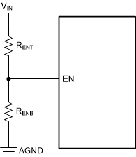
BehaviorRemote precision undervoltage lockout can be implemented with this functionality as shown in Figure 7-2. See Section 8.2.2.8 for component selection.
 Figure 7-2 VIN Undervoltage
Lockout
 Using the EN/UVLO Pin
The high-voltage compliant EN/UVLO pin can be connected directly to the VIN input pin if remote precision control is not needed. The EN/UVLO pin must not be allowed to float. The various EN threshold parameters are listed in the Section 6.5. Figure 7-1 shows the precision enable behavior. After EN/UVLO goes above VEN-VOUT with a delay of about 1 ms, the output voltage begins to rise with a soft-start and reaches close to the final value in about 2.58 ms (tss). After a delay of about 2 ms (tPGOOD_ACT), the PGOOD flag goes high. During startup, the device is not allowed to enter FPWM mode until the soft-start time has elapsed. Check Section 8.2.2.8 for component selection.