SLVSEX5A October 2020 – December 2020 TPSM41615
PRODUCTION DATA
- 1 Features
- 2 Applications
- 3 Description
- 4 Revision History
- 5 Pin Configuration and Functions
- 6 Specifications
-
7 Detailed Description
- 7.1 Overview
- 7.2 Functional Block Diagram
- 7.3
Feature Description
- 7.3.1 Setting the Output Voltage
- 7.3.2 RS+/RS- Remote Sense Function
- 7.3.3 Ramp Select (RAMP and RAMP_SEL)
- 7.3.4 Switching Frequency (RT)
- 7.3.5 Synchronization (SYNC)
- 7.3.6 Stand-alone/Stackable Operation
- 7.3.7 Improved Transient Performance versus Fixed Frequency (Stand-alone Operation Only)
- 7.3.8 Output On/Off Enable (EN)
- 7.3.9 Power Good (PGOOD)
- 7.3.10 Soft-Start Operation
- 7.3.11 Input Capacitor Selection
- 7.3.12 Output Capacitor Selection
- 7.3.13 Current Limit (ILIM)
- 7.3.14 Safe Start-up into Pre-Biased Outputs
- 7.3.15 Overcurrent Protection
- 7.3.16 Output Overvoltage and Undervoltage Protection
- 7.3.17 Overtemperature Protection
- 7.4 Device Functional Modes
- 8 Application and Implementation
- 9 Power Supply Recommendations
- 10Layout
- 11Device and Documentation Support
- 12Mechanical, Packaging, and Orderable Information
Package Options
Mechanical Data (Package|Pins)
- MOV|69
Thermal pad, mechanical data (Package|Pins)
Orderable Information
8.2.3 Application Curves
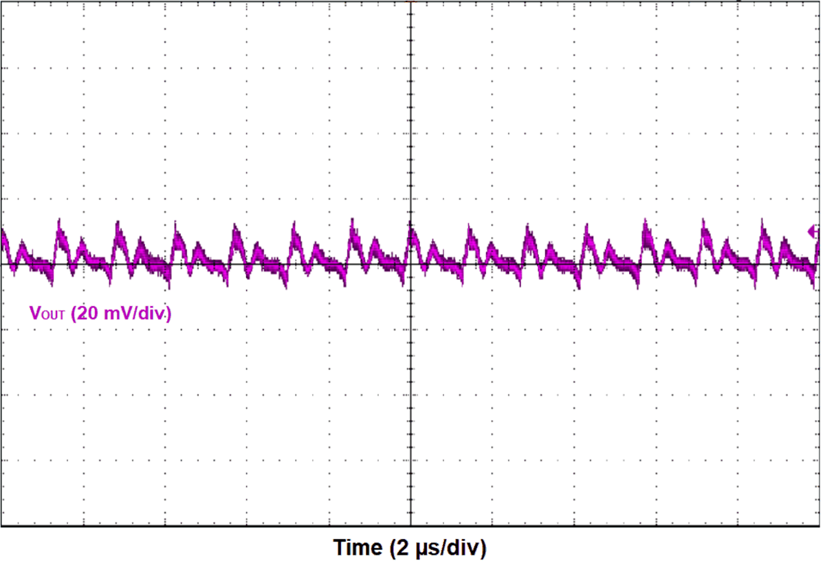
 Figure 8-2 Output Ripple Waveform
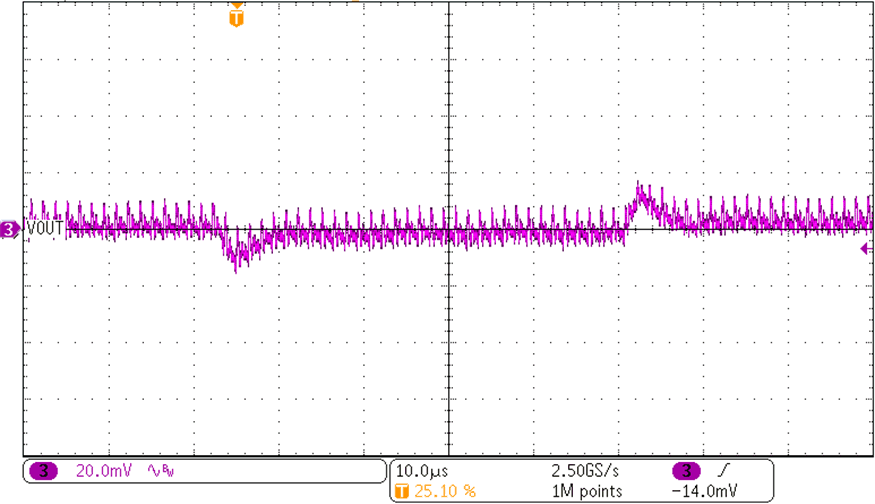
 Figure 8-4 5-A Transient Load Step
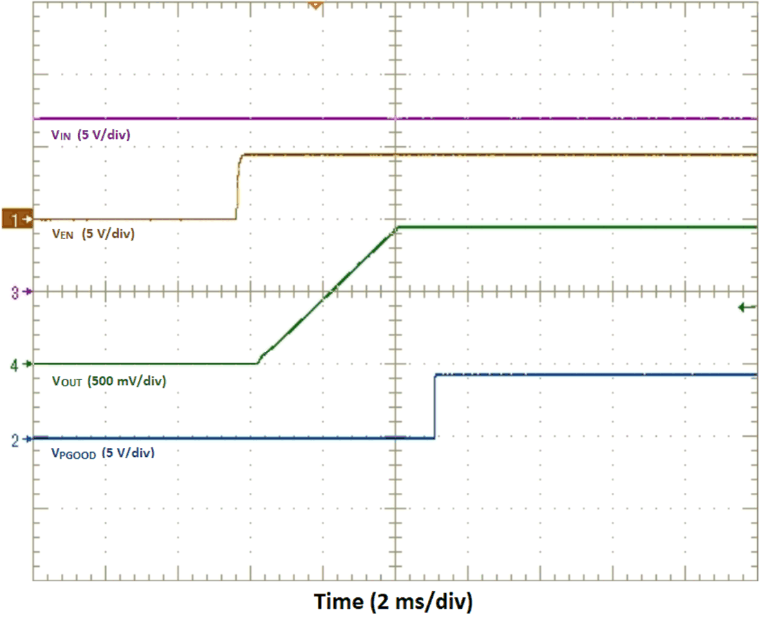
 Figure 8-3 Start-Up Waveforms
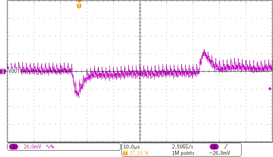
 Figure 8-5 10-A
Transient Load Step