SLVSEW0A September 2020 – December 2020 TPSM41625
PRODUCTION DATA
- 1 Features
- 2 Applications
- 3 Description
- 4 Revision History
- 5 Pin Configuration and Functions
- 6 Specifications
-
7 Detailed Description
- 7.1 Overview
- 7.2 Functional Block Diagram
- 7.3
Feature Description
- 7.3.1 Setting the Output Voltage
- 7.3.2 Output Voltage Current Rating
- 7.3.3 RS+/RS- Remote Sense Function
- 7.3.4 Ramp Select (RAMP and RAMP_SEL)
- 7.3.5 Switching Frequency (RT)
- 7.3.6 Synchronization (SYNC)
- 7.3.7 Stand-alone/Stackable Operation
- 7.3.8 Improved Transient Performance versus Fixed Frequency (Stand-alone Operation Only)
- 7.3.9 Output On/Off Enable (EN)
- 7.3.10 Power Good (PGOOD)
- 7.3.11 Soft-Start Operation
- 7.3.12 Input Capacitor Selection
- 7.3.13 Output Capacitor Selection
- 7.3.14 Current Limit (ILIM)
- 7.3.15 Safe Start-up into Pre-Biased Outputs
- 7.3.16 Overcurrent Protection
- 7.3.17 Output Overvoltage and Undervoltage Protection
- 7.3.18 Overtemperature Protection
- 7.4 Device Functional Modes
- 8 Application and Implementation
- 9 Power Supply Recommendations
- 10Layout
- 11Device and Documentation Support
- 12Mechanical, Packaging, and Orderable Information
Package Options
Mechanical Data (Package|Pins)
- MOV|69
Thermal pad, mechanical data (Package|Pins)
Orderable Information
3 Description
The TPSM41625 power module is an easy-to-use integrated power supply that combines a DC/DC converter with power MOSFETs, a shielded inductor, and passives into a compact QFN package. This power solution requires few external components while maintaining the ability to adjust key parameters to meet specific design requirements. Applications requiring increased current can benefit from the ability to parallel two TPSM41625 devices.
The 11-mm × 16-mm × 4.2-mm, 69-pin QFN package with optimal package layout has excellent power dissipation capability which enhances thermal performance. The package footprint has all signal pins accessible from the perimeter and large thermal pads beneath the device. The TPSM41625 offers flexibilty with many features including power good signal, clock synchronization, programmable UVLO, soft-start timing selection, prebias start-up, as well as overcurrent and overtemperature protection making it a great product for powering a wide range of devices and systems.
| DEVICE NUMBER | PACKAGE(1) | BODY SIZE (NOM) |
|---|---|---|
| TPSM41625 | QFN (69) | 11 mm × 16 mm |
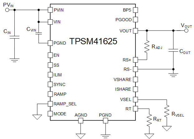
 Simplified Schematic
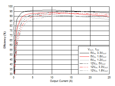
 Typical Efficiency