SNVSBD0B December 2019 – September 2021 TPSM53602
PRODUCTION DATA
- 1 Features
- 2 Applications
- 3 Description
- 4 Revision History
- 5 Pin Configuration and Functions
- 6 Specifications
-
7 Detailed Description
- 7.1 Overview
- 7.2 Functional Block Diagram
- 7.3
Feature Description
- 7.3.1 Adjusting the Output Voltage
- 7.3.2 Switching Frequency
- 7.3.3 Input Capacitors
- 7.3.4 Output Capacitors
- 7.3.5 Output On/Off Enable (EN)
- 7.3.6 Programmable Undervoltage Lockout (UVLO)
- 7.3.7 Power Good (PGOOD)
- 7.3.8 Light Load Operation
- 7.3.9 Voltage Dropout
- 7.3.10 Overcurrent Protection (OCP)
- 7.3.11 Thermal Shutdown
- 7.4 Device Functional Modes
- 8 Application and Implementation
- 9 Power Supply Recommendations
- 10Layout
- 11Device and Documentation Support
- 12Mechanical, Packaging, and Orderable Information
Package Options
Mechanical Data (Package|Pins)
- RDA|15
Thermal pad, mechanical data (Package|Pins)
Orderable Information
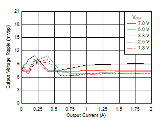
6.8 Typical Characteristics (VIN = 24 V)
The typical characteristic data has been developed from actual products tested at TA = 25°C. This data is considered typical for the device.

| VIN = 24 V |

| VIN = 24 V |

| VIN = 24 V | VOUT ≤ 1.8 V | |
| PCB = 85-mm × 65-mm, 4-layer, 2-oz. copper | ||

| VIN = 24 V |

| VIN = 24 V | COUT = 4x 47µF | ||

| VIN = 24 V | VOUT = 5 V | ||
| PCB = 85-mm × 65-mm, 4-layer, 2-oz. copper | |||