SNVSBD0B December 2019 – September 2021 TPSM53602
PRODUCTION DATA
- 1 Features
- 2 Applications
- 3 Description
- 4 Revision History
- 5 Pin Configuration and Functions
- 6 Specifications
-
7 Detailed Description
- 7.1 Overview
- 7.2 Functional Block Diagram
- 7.3
Feature Description
- 7.3.1 Adjusting the Output Voltage
- 7.3.2 Switching Frequency
- 7.3.3 Input Capacitors
- 7.3.4 Output Capacitors
- 7.3.5 Output On/Off Enable (EN)
- 7.3.6 Programmable Undervoltage Lockout (UVLO)
- 7.3.7 Power Good (PGOOD)
- 7.3.8 Light Load Operation
- 7.3.9 Voltage Dropout
- 7.3.10 Overcurrent Protection (OCP)
- 7.3.11 Thermal Shutdown
- 7.4 Device Functional Modes
- 8 Application and Implementation
- 9 Power Supply Recommendations
- 10Layout
- 11Device and Documentation Support
- 12Mechanical, Packaging, and Orderable Information
Package Options
Mechanical Data (Package|Pins)
- RDA|15
Thermal pad, mechanical data (Package|Pins)
Orderable Information
7.4.2 Auto Mode
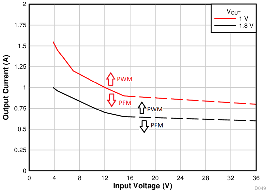
In auto mode, the device moves between Pulse-Width Modulation (PWM) and Pulse-Frequency Modulation (PFM) as the load changes. At light loads, the regulator operates in PFM mode. At higher loads, the mode changes to PWM mode. The typical load current for which the device moves from PFM to PWM can be found in Figure 7-14 and Figure 7-15. The output current at which the device changes modes depends on the input voltage and the output voltage. For output currents above the curve, the device is in PWM mode. If the curve is a solid line, the PWM switching frequency is 1.4 MHz nominal. If the curve is a dashed line, the PWM switching frequency is reduced due to the minimum on-time of the internal controller to maintain output voltage regulation. For currents below the curves, the device is in PFM mode. For applications where the switching frequency must be known for a given condition, the above mentioned effects must be carefully tested before the design is finalized.
In PWM mode, the regulator operates at a constant frequency using PWM to regulate the output voltage. While operating in this mode, the output voltage is regulated by switching at a constant frequency and modulating the duty cycle to control the power to the load. This provides excellent line and load regulation and low output voltage ripple.
In PFM mode, the high-side MOSFET is turned on in a burst of one or more pulses to provide energy to the load. The duration of the burst and the actual switching frequency depends on the input voltage, output voltage, and load current. The frequency of these bursts is adjusted to regulate the output while diode emulation is used to maximize efficiency. This mode provides high light-load efficiency by reducing the amount of input supply current required to regulate the output voltage at small loads. However, in this mode, expect larger output voltage ripple and variable switching frequency.
 Figure 7-14 PFM/PWM Thresholds (3.3 V,
5 V, and 7 V)
 Figure 7-15 PFM/PWM Thresholds (1 V
and 1.8 V)