SNVSBC9C November 2019 – September 2021 TPSM53604
PRODUCTION DATA
- 1 Features
- 2 Applications
- 3 Description
- 4 Revision History
- 5 Pin Configuration and Functions
- 6 Specifications
-
7 Detailed Description
- 7.1 Overview
- 7.2 Functional Block Diagram
- 7.3
Feature Description
- 7.3.1 Adjusting the Output Voltage
- 7.3.2 Switching Frequency
- 7.3.3 Input Capacitors
- 7.3.4 Output Capacitors
- 7.3.5 Output On/Off Enable (EN)
- 7.3.6 Programmable Undervoltage Lockout (UVLO)
- 7.3.7 Power Good (PGOOD)
- 7.3.8 Light Load Operation
- 7.3.9 Voltage Dropout
- 7.3.10 Overcurrent Protection (OCP)
- 7.3.11 Thermal Shutdown
- 7.4 Device Functional Modes
- 8 Application and Implementation
- 9 Power Supply Recommendations
- 10Layout
- 11Device and Documentation Support
- 12Mechanical, Packaging, and Orderable Information
Package Options
Mechanical Data (Package|Pins)
- RDA|15
Thermal pad, mechanical data (Package|Pins)
Orderable Information
7.3.9 Voltage Dropout
Voltage dropout is the difference between the input voltage and output voltage that is required to maintain output voltage regulation while providing the rated output current.
To ensure the TPSM53604 maintains output voltage regulation over the operating temperature range, the minimum VIN is 3.8 V or (VOUT + 1 V), whichever is greater.
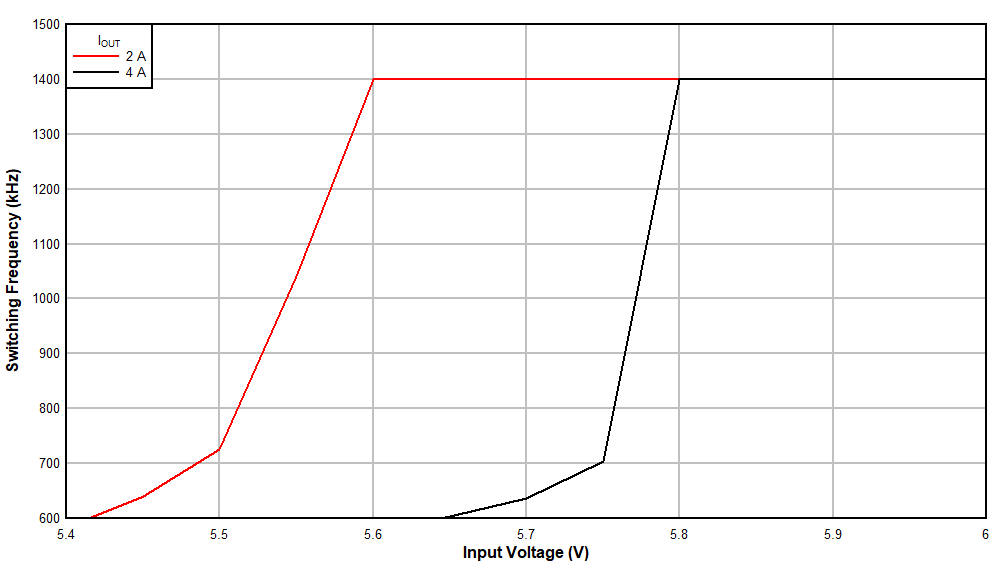
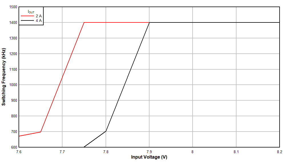
The TPSM53604 operates in a frequency foldback mode when the dropout voltage is less than the recommendation above. Frequency foldback reduces the switching frequency to allow the output voltage to maintain regulation as input voltage decreases. At light load, the TPSM53604 operates in PFM mode which is a reduced frequency operation, see Section 7.4.2 for more information on PFM mode. Figure 7-7 through Figure 7-12 show typical dropout voltage and frequency foldback curves for 3.3 V, 5 V, and 7 V outputs at TA = 25°C.
As ambient temperature increases, dropout voltage and frequency foldback occur at higher input voltage.
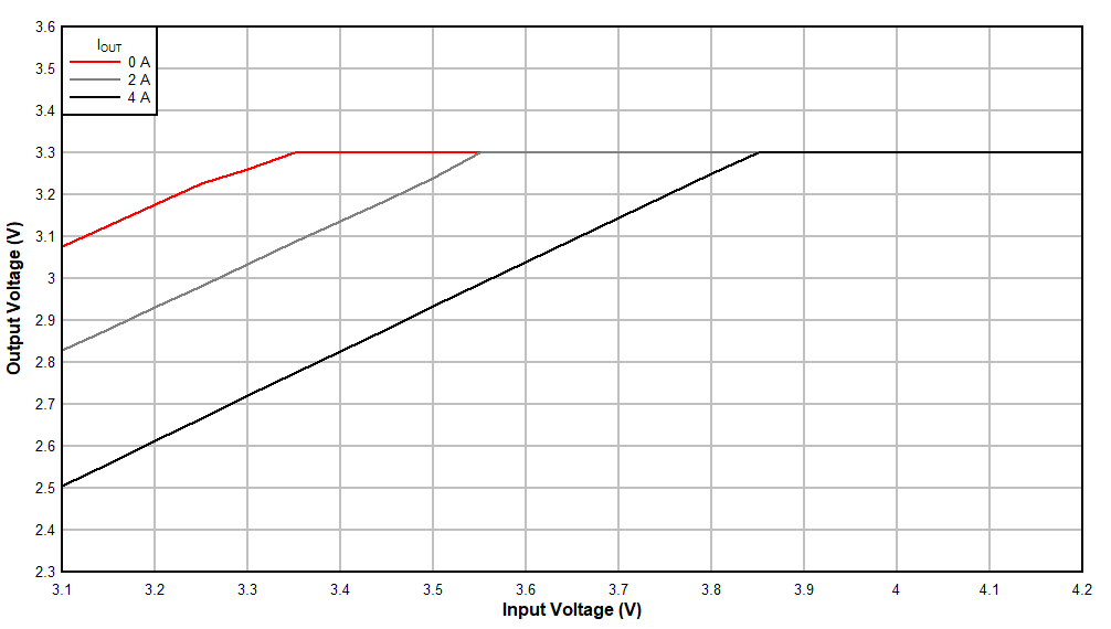
| VOUT = 3.3 V |
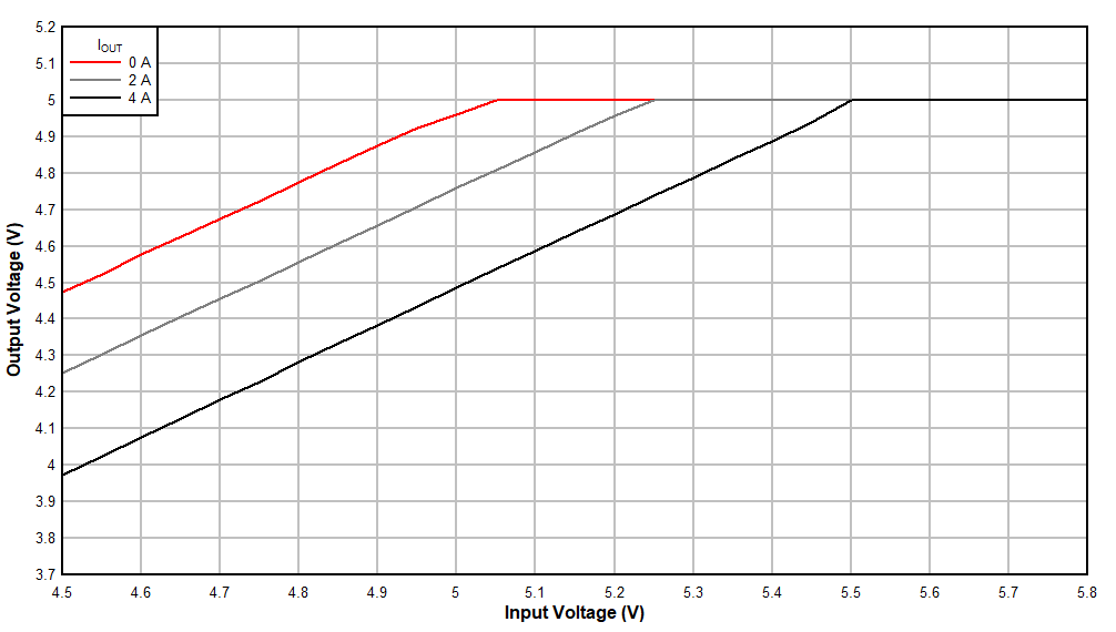
| VOUT = 5 V |
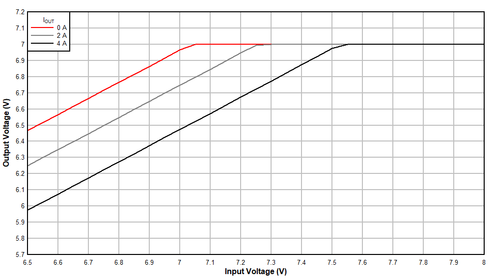
| VOUT = 7 V |
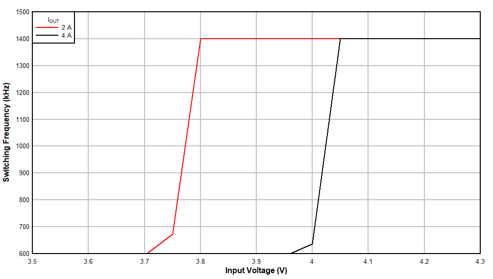
| VOUT = 3.3 V |
| VOUT = 5 V |
| VOUT = 7 V |