SLVSFI4B December   2020  – October 2021 TPSM5601R5H , TPSM5601R5HE

PRODUCTION DATA  

  1. Features
  2. Applications
  3. Description
  4. Revision History
  5. Device Comparison Table
  6. Pin Configuration and Functions
  7. Specifications
    1. 7.1 Absolute Maximum Ratings
    2. 7.2 ESD Ratings
    3. 7.3 Recommended Operating Conditions
    4. 7.4 Thermal Information
    5. 7.5 Electrical Characteristics
    6. 7.6 Typical Characteristics (VIN = 12 V)
    7. 7.7 Typical Characteristics (VIN = 24 V)
    8. 7.8 Typical Characteristics (VIN = 48 V)
    9. 7.9 Typical Characteristics (VIN = 60 V)
  8. Detailed Description
    1. 8.1 Overview
    2. 8.2 Functional Block Diagram
    3. 8.3 Feature Description
      1. 8.3.1 Adjustable Output Voltage (FB)
      2. 8.3.2 Minimum Input Capacitance
      3. 8.3.3 Minimum Output Capacitance
      4. 8.3.4 Precision Enable (EN), Undervoltage Lockout (UVLO), and Hysteresis (HYS)
      5. 8.3.5 Power Good (PGOOD)
      6. 8.3.6 Spread Spectrum Operation
      7. 8.3.7 Overcurrent Protection (OCP)
      8. 8.3.8 Thermal Shutdown
    4. 8.4 Device Functional Modes
      1. 8.4.1 Active Mode
      2. 8.4.2 Standby Mode
      3. 8.4.3 Shutdown Mode
  9. Applications and Implementation
    1. 9.1 Application Information
    2. 9.2 Typical Application
      1. 9.2.1 Design Requirements
      2. 9.2.2 Detailed Design Procedure
        1. 9.2.2.1 Custom Design With WEBENCH® Tools
        2. 9.2.2.2 Output Voltage Setpoint
        3. 9.2.2.3 Input Capacitors
        4. 9.2.2.4 Output Capacitor Selection
        5. 9.2.2.5 Power Good Signal
      3. 9.2.3 Application Curves
  10. 10Power Supply Recommendations
  11. 11Layout
    1. 11.1 Layout Guidelines
    2. 11.2 Layout Example
      1. 11.2.1 Theta JA versus PCB Area
      2. 11.2.2 Package Specifications
      3. 11.2.3 EMI
        1. 11.2.3.1 EMI Plots
  12. 12Device and Documentation Support
    1. 12.1 Device Support
      1. 12.1.1 Third-Party Products Disclaimer
      2. 12.1.2 Development Support
        1. 12.1.2.1 Custom Design With WEBENCH® Tools
    2. 12.2 Documentation Support
      1. 12.2.1 Related Documentation
    3. 12.3 Receiving Notification of Documentation Updates
    4. 12.4 Support Resources
    5. 12.5 Trademarks
    6. 12.6 Electrostatic Discharge Caution
    7. 12.7 Glossary
  13. 13Mechanical, Packaging, and Orderable Information

Package Options

Mechanical Data (Package|Pins)
Thermal pad, mechanical data (Package|Pins)
Orderable Information

Typical Characteristics (VIN = 24 V)

TA = 25°C, unless otherwise noted.
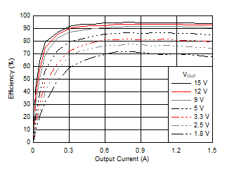
GUID-20201030-CA0I-Q2SB-L8HQ-LS21SDBM96L7-low.gifFigure 7-7 Efficiency
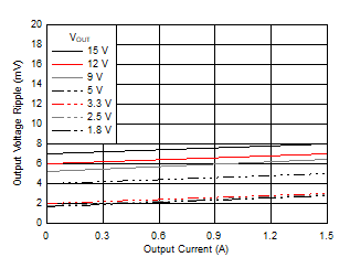
GUID-20201116-CA0I-CZ09-RHK5-PD1BH7NHM80M-low.gif
COUT = 2 × 47-µF, 25-V, ceramic
Figure 7-9 Output Voltage Ripple
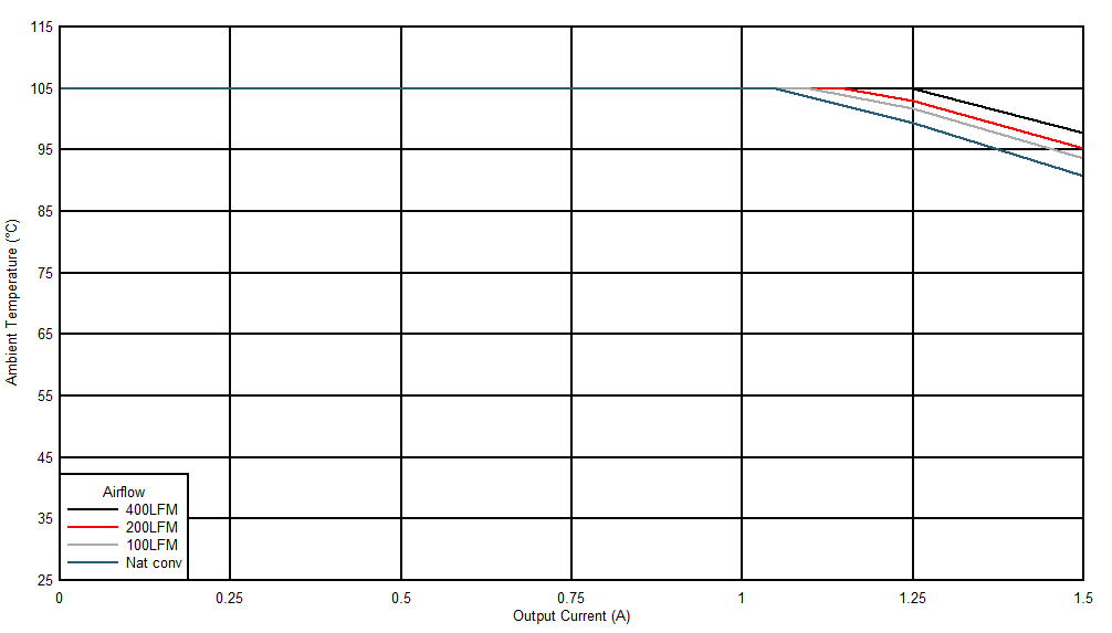
GUID-20201116-CA0I-BBF5-LW9R-TKLHB6NXFNR3-low.gif
Device soldered to a 63.5-mm × 82.5-mm, 4-layer PCB
Figure 7-11 Safe Operating Area (VOUT = 5.0 V)
GUID-20201030-CA0I-FKLP-D3DR-GQ31HSNQXKCX-low.gifFigure 7-8 Power Dissipation
GUID-20201116-CA0I-X2WD-3BSH-5JPGKPCKGXFN-low.gif
Device soldered to a 63.5-mm × 82.5-mm, 4-layer PCB
Figure 7-10 Safe Operating Area (VOUT = 1.8 V)
GUID-20201116-CA0I-MWV3-J2SR-GPWBKGGXWT1Z-low.gif
Device soldered to a 63.5-mm × 82.5-mm, 4-layer PCB
Figure 7-12 Safe Operating Area (VOUT = 12 V)