SLUSEP8 January 2022 TPSM5D1806E
PRODUCTION DATA
- 1 Features
- 2 Applications
- 3 Description
- 4 Revision History
- 5 Pin Configuration and Functions
- 6 Specifications
-
7 Detailed Description
- 7.1 Overview
- 7.2 Functional Block Diagram
- 7.3
Feature Description
- 7.3.1 Adjustable Output Voltage
- 7.3.2 Frequency Selection
- 7.3.3 Minimum and Maximum Input Voltage
- 7.3.4 Recommended Settings
- 7.3.5 Device Mode Configuration
- 7.3.6 Input Capacitors
- 7.3.7 Minimum Required Output Capacitance
- 7.3.8 Ambient Temperature Versus Total Power Dissipation
- 7.3.9 Remote Sense
- 7.3.10 Enable (EN) and Undervoltage Lockout (UVLO)
- 7.3.11 Soft Start
- 7.3.12 Power Good
- 7.3.13 Safe Start-Up into Pre-Biased Outputs
- 7.3.14 BP5
- 7.3.15 Overcurrent Protection
- 7.3.16 Thermal Shutdown
- 7.4 Device Functional Modes
- 8 Application and Implementation
- 9 Power Supply Recommendations
- 10Layout
- 11Device and Documentation Support
- 12Mechanical, Packaging, and Orderable Information
Package Options
Mechanical Data (Package|Pins)
- RDB|51
Thermal pad, mechanical data (Package|Pins)
Orderable Information
7.3.3 Minimum and Maximum Input Voltage
The minimum input voltage of the TPSM5D1806E is 4.5 V, however, the minimum recommended input voltage increases at higher output voltages. Refer to Table 7-2 to determine the minimum recommended input voltage for each switching frequency. Also reference Table 7-1 to ensure that the output voltage can be operated at the selected switching frequency. Control the turn ON and turn OFF of the device at an input voltage greater than the minimum using a resistor divider on the EN1 (EN2) pin between VIN and AGND (see Section 7.3.10).
| Switching Frequency (kHz) | Minimum Input Voltage |
|---|---|
| 500 | 4.5 V |
| 1000 | 4.5 V or VOUT × 1.3 (whichever is greater) |
| 1500 | 4.5 V or VOUT × 1.6 (whichever is greater) |
| 2000 | 4.5 V or VOUT × 1.75 (whichever is greater) |
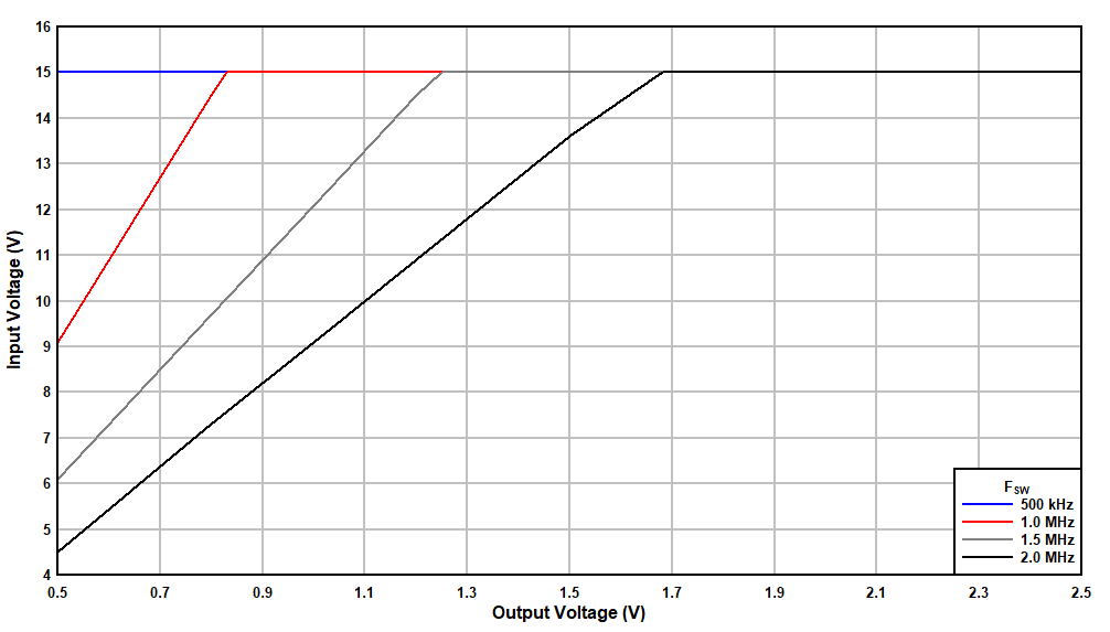
Additionally, the maximum input voltage of the TPSM5D1806E is 15 V, however, the maximum recommended input voltage decreases at lower output voltages and higher switching frequencies. See Figure 7-3 for the maximum recommended input voltage for each of the allowable switching frequencies across the output voltage range.
 Figure 7-3 Maximum Input Voltage