SLUSEP8 January 2022 TPSM5D1806E
PRODUCTION DATA
- 1 Features
- 2 Applications
- 3 Description
- 4 Revision History
- 5 Pin Configuration and Functions
- 6 Specifications
-
7 Detailed Description
- 7.1 Overview
- 7.2 Functional Block Diagram
- 7.3
Feature Description
- 7.3.1 Adjustable Output Voltage
- 7.3.2 Frequency Selection
- 7.3.3 Minimum and Maximum Input Voltage
- 7.3.4 Recommended Settings
- 7.3.5 Device Mode Configuration
- 7.3.6 Input Capacitors
- 7.3.7 Minimum Required Output Capacitance
- 7.3.8 Ambient Temperature Versus Total Power Dissipation
- 7.3.9 Remote Sense
- 7.3.10 Enable (EN) and Undervoltage Lockout (UVLO)
- 7.3.11 Soft Start
- 7.3.12 Power Good
- 7.3.13 Safe Start-Up into Pre-Biased Outputs
- 7.3.14 BP5
- 7.3.15 Overcurrent Protection
- 7.3.16 Thermal Shutdown
- 7.4 Device Functional Modes
- 8 Application and Implementation
- 9 Power Supply Recommendations
- 10Layout
- 11Device and Documentation Support
- 12Mechanical, Packaging, and Orderable Information
Package Options
Mechanical Data (Package|Pins)
- RDB|51
Thermal pad, mechanical data (Package|Pins)
Orderable Information
10.2.2 EMI
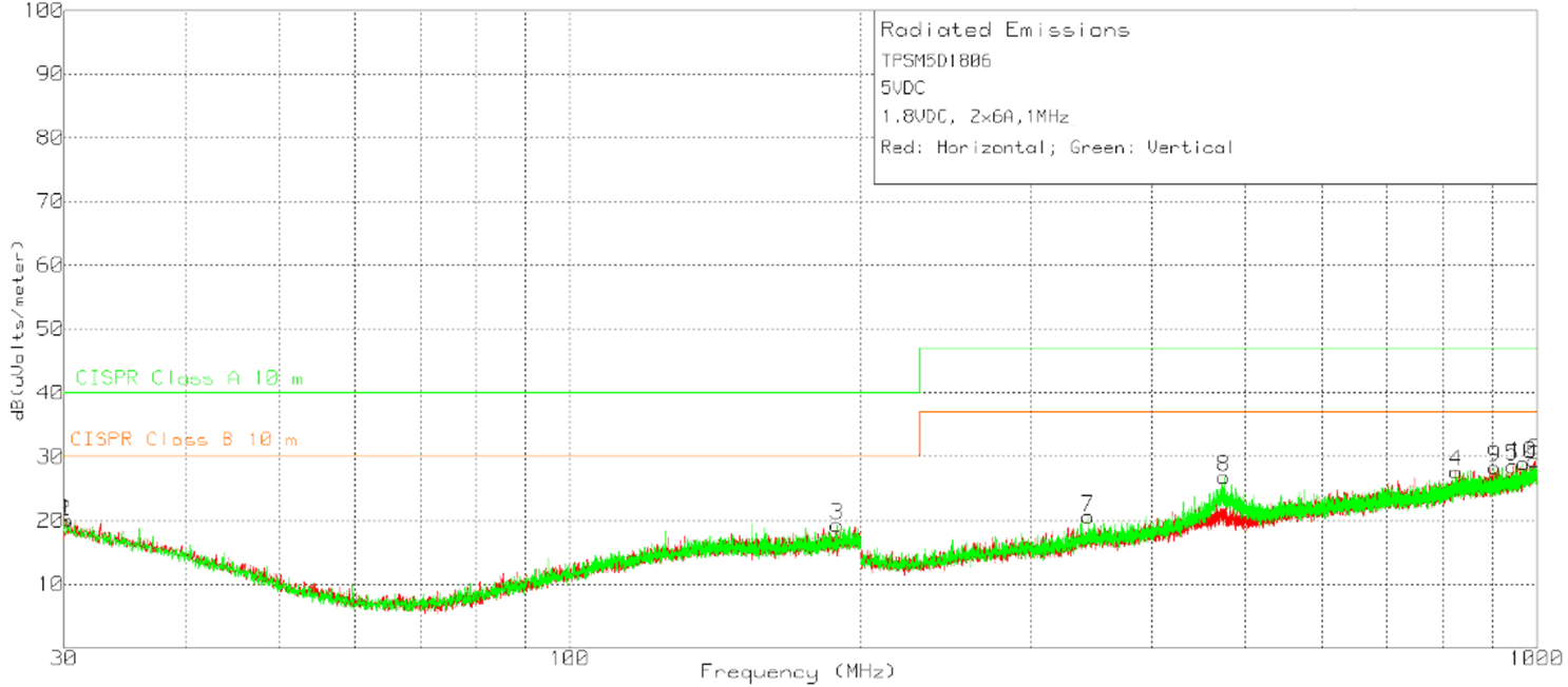
The TPSM5D1806E is compliant with EN55011 Class-B radiated emissions. Figure 10-3 and Figure 10-4 show typical examples of radiated emissions plots for the TPSM5D1806E. The graphs include the plots of the antenna in the horizontal and vertical positions.
EMI plots were measured using the standard TPSM5D1806EVM with ferrite beads (Murata, BLM18SG330SN1) in series with the input wires.
 Figure 10-3 Radiated Emissions 5-V Input, 1.8-V Outputs, 6-A/Output Load
 Figure 10-4 Radiated Emissions 12-V Input, 5-V Output, 6-A/Output Load