SLVSH65A February 2023 – November 2023 TPSM63610E
PRODUCTION DATA
- 1
- 1 Features
- 2 Applications
- 3 Description
- 4 Revision History
- 5 Device Comparison Table
- 6 Pin Configuration and Functions
- 7 Specifications
-
8 Detailed Description
- 8.1 Overview
- 8.2 Functional Block Diagram
- 8.3
Feature Description
- 8.3.1 Input Voltage Range (VIN1, VIN2)
- 8.3.2 Adjustable Output Voltage (FB)
- 8.3.3 Input Capacitors
- 8.3.4 Output Capacitors
- 8.3.5 Switching Frequency (RT)
- 8.3.6 Precision Enable and Input Voltage UVLO (EN)
- 8.3.7 Frequency Synchronization (SYNC/MODE)
- 8.3.8 Spread Spectrum
- 8.3.9 Power-Good Monitor (PG)
- 8.3.10 Adjustable Switch-Node Slew Rate (RBOOT, CBOOT)
- 8.3.11 Bias Supply Regulator (VCC, VLDOIN)
- 8.3.12 Overcurrent Protection (OCP)
- 8.3.13 Thermal Shutdown
- 8.4 Device Functional Modes
-
9 Applications and Implementation
- 9.1 Application Information
- 9.2
Typical Applications
- 9.2.1 Design 1 – High-Efficiency 8-A (10-A peak) Synchronous Buck Regulator for Industrial Applications
- 9.2.2 Design 2 – Inverting Buck-Boost Regulator with Negative Output Voltage
- 9.3 Power Supply Recommendations
- 9.4 Layout
- 10Device and Documentation Support
- 11Mechanical, Packaging, and Orderable Information
Package Options
Mechanical Data (Package|Pins)
- RDF|22
Thermal pad, mechanical data (Package|Pins)
Orderable Information
8.3.8 Spread Spectrum
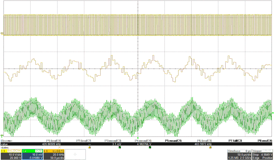
Spread spectrum is configurable using the SPSP pin. Spread spectrum eliminates peak emissions at specific frequencies by spreading these peaks across a wider range of frequencies than a part with fixed-frequency operation. The TPSM63610E implements a modulation pattern designed to reduce low frequency-conducted emissions from the first few harmonics of the switching frequency. The pattern can also help reduce the higher harmonics that are more difficult to filter, which can fall in the FM band. These harmonics often couple to the environment through electric fields around the switch node and inductor. The TPSM63610E uses a ±4% (typical) spread of frequencies which can spread energy smoothly across the FM and TV bands. The device implements Dual Random Spread Spectrum (DRSS). DRSS is a combination of a triangular frequency spreading pattern and pseudorandom frequency hopping. The combination allows the spread spectrum to be very effective at spreading the energy at the following:
- Fundamental switching harmonic with slow triangular pattern
- High frequency harmonics with additional psuedorandom jumps at the switching frequency
 Figure 8-3 Output Ripple Without
Ripple Cancellation Showing VSW (Top), FSW (Middle),
VOUT (Bottom)
 Figure 8-4 Output Ripple with Ripple
Cancellation Showing VSW (Top), FSW (Middle),
VOUT (Bottom)
Figure 8-4 Output Ripple with Ripple
Cancellation Showing VSW (Top), FSW (Middle),
VOUT (Bottom)The spread spectrum is only available while the clock of the TPSM63610E are free running at their natural frequency. Any of the following conditions overrides spread spectrum, turning it off:
- The clock is slowed due to operation at low input voltage. This is operation in dropout.
- The clock is slowed under light load in auto mode. This is normally not seen above 750-mA load. Note that if the device is operating in FPWM mode, spread spectrum is active, even if there is no load.
- The clock is slowed due to high input-to-output voltage ratio. This mode of operation is expected if on-time reaches minimum on time.