SLVSHL0D June 2024 – December 2024 TPSM81033
PRODUCTION DATA
- 1
- 1 Features
- 2 Applications
- 3 Description
- 4 Pin Configuration and Functions
- 5 Specifications
-
6 Detailed Description
- 6.1 Overview
- 6.2 Functional Block Diagram
- 6.3
Feature Description
- 6.3.1 Undervoltage Lockout
- 6.3.2 Enable and Soft Start
- 6.3.3 Setting the Output Voltage
- 6.3.4 Current Limit Operation
- 6.3.5 Pass-Through Operation
- 6.3.6 Power Good Indicator
- 6.3.7 Implement Output Discharge by PG function
- 6.3.8 Overvoltage Protection
- 6.3.9 Output Short-to-Ground Protection
- 6.3.10 Thermal Shutdown
- 6.4 Device Functional Modes
- 7 Application and Implementation
- 8 Device and Documentation Support
- 9 Revision History
- 10Mechanical, Packaging, and Orderable Information
Package Options
Mechanical Data (Package|Pins)
- VCD|9
Thermal pad, mechanical data (Package|Pins)
Orderable Information
7.4.3 Thermal Considerations
Restrict the maximum IC junction temperature to 125°C under normal operating conditions. Calculate the maximum allowable dissipation, PD(max), and keep the actual power dissipation less than or equal to PD(max). The maximum-power-dissipation limit is determined using Equation 8.
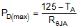
where
- TA is the maximum ambient temperature for the application
- RθJA is the junction-to-ambient thermal resistance given in Thermal Information.
The TPSM81033 comes in a QFN package. The real junction-to-ambient thermal resistance of the package greatly depends on the PCB type, layout. Using larger and thicker PCB copper for the power pads (GND, PVIN, and VOUT) to enhance the thermal performance. Using more vias connects the ground plate on the top layer and bottom layer around the IC without solder mask also improves the thermal capability.