SLVSHL0D June 2024 – December 2024 TPSM81033
PRODUCTION DATA
- 1
- 1 Features
- 2 Applications
- 3 Description
- 4 Pin Configuration and Functions
- 5 Specifications
-
6 Detailed Description
- 6.1 Overview
- 6.2 Functional Block Diagram
- 6.3
Feature Description
- 6.3.1 Undervoltage Lockout
- 6.3.2 Enable and Soft Start
- 6.3.3 Setting the Output Voltage
- 6.3.4 Current Limit Operation
- 6.3.5 Pass-Through Operation
- 6.3.6 Power Good Indicator
- 6.3.7 Implement Output Discharge by PG function
- 6.3.8 Overvoltage Protection
- 6.3.9 Output Short-to-Ground Protection
- 6.3.10 Thermal Shutdown
- 6.4 Device Functional Modes
- 7 Application and Implementation
- 8 Device and Documentation Support
- 9 Revision History
- 10Mechanical, Packaging, and Orderable Information
Package Options
Mechanical Data (Package|Pins)
- VCD|9
Thermal pad, mechanical data (Package|Pins)
Orderable Information
7.2.2.1 Setting the Output Voltage
TPSM81033 support the fixed 5V output voltage when FB is connected to AVIN, which can provide better load regulation performance.
For other output voltage, the output voltage is set by an external resistor divider (R1, R2 in Figure 7-2). When the output voltage is regulated, the typical voltage at the FB pin is VREF. Thus the resistor divider is determined by Equation 5.
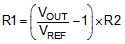
where
- VOUT is the regulated output voltage
- VREF is the internal reference voltage at the FB pin
For the best accuracy, keep R2 smaller than 300kΩ to ensure the current flowing through R2 is at least 100 times larger than the FB pin leakage current. Changing R2 towards a lower value increases the immunity against noise injection. Changing the R2 towards a higher value reduces the quiescent current for achieving highest efficiency at low load currents.
 Figure 7-2 Coin Battery to
3.3V Boost Converter
Figure 7-2 Coin Battery to
3.3V Boost Converter