SLVSDT1C July   2017  – June 2020 TPSM82480

PRODUCTION DATA.  

  1. Features
  2. Applications
  3. Description
    1.     Device Images
      1.      Typical Application space
      2.      Efficiency vs Output Current space space
  4. Revision History
  5. Pin Configuration and Functions
    1.     Pin Functions
  6. Specifications
    1. 6.1 Absolute Maximum Ratings
    2. 6.2 ESD Ratings
    3. 6.3 Recommended Operating Conditions
    4. 6.4 Thermal Information
    5. 6.5 Electrical Characteristics
    6. 6.6 Typical Characteristics
  7. Detailed Description
    1. 7.1 Overview
    2. 7.2 Functional Block Diagram
    3. 7.3 Feature Description
      1. 7.3.1  Enable and Shutdown (EN)
      2. 7.3.2  Soft-Start (SS), Pre-biased Output
      3. 7.3.3  Tracking (TR)
      4. 7.3.4  Output Voltage Select (VSEL)
      5. 7.3.5  Forced PWM (MODE)
      6. 7.3.6  Power Good (PG)
      7. 7.3.7  Thermal Good (TG)
      8. 7.3.8  Active Output Discharge
      9. 7.3.9  Undervoltage Lockout (UVLO)
      10. 7.3.10 Thermal Shutdown
    4. 7.4 Device Functional Modes
      1. 7.4.1 Pulse Width Modulation (PWM) Operation
      2. 7.4.2 Power Save Mode (PSM) Operation
      3. 7.4.3 Minimum Duty Cycle and 100% Mode Operation
      4. 7.4.4 Phase Shifted Operation
      5. 7.4.5 Phase Add/Shed and Current Balancing
      6. 7.4.6 Current Limit and Short Circuit Protection
  8. Application and Implementation
    1. 8.1 Application Information
    2. 8.2 Typical Application
      1. 8.2.1 Design Requirements
      2. 8.2.2 Detailed Design Procedure
        1. 8.2.2.1 Setting the Output Voltage
        2. 8.2.2.2 Setting VOUT2 Using the VSEL Feature
        3. 8.2.2.3 Feedforward Capacitance
        4. 8.2.2.4 Output Capacitor Selection
        5. 8.2.2.5 Input Capacitor Selection
        6. 8.2.2.6 Soft-Start Capacitor Selection
        7. 8.2.2.7 Tracking
        8. 8.2.2.8 Thermal Good
      3. 8.2.3 Application Curves
    3. 8.3 System Examples
  9. Power Supply Recommendations
  10. 10Layout
    1. 10.1 Layout Guidelines
    2. 10.2 Layout Example
  11. 11Device and Documentation Support
    1. 11.1 Documentation Support
      1. 11.1.1 Related Documentation
    2. 11.2 Receiving Notification of Documentation Updates
    3. 11.3 Community Resources
    4. 11.4 Trademarks
    5. 11.5 Electrostatic Discharge Caution
    6. 11.6 Glossary
  12. 12Mechanical, Packaging, and Orderable Information
    1. 12.1 Tape and Reel Information

Package Options

Mechanical Data (Package|Pins)
Thermal pad, mechanical data (Package|Pins)
Orderable Information

Application Curves

VIN= 3.6 V, VOUT = 1.8V (R1 / R2 = 240 kΩ / 120 kΩ), TA = 25°C, MODE = Low, (unless otherwise noted)
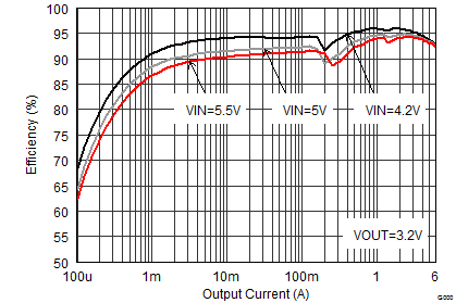
TPSM82480 SLVSDT1_eff32_iout.gif
VOUT = 3.2 V
Figure 10. Efficiency vs Output Current
TPSM82480 SLVSDT1_eff18_iout.gif
VOUT = 1.8 V
Figure 12. Efficiency vs Output Current
TPSM82480 SLVSDT1_eff09_iout.gif
VOUT = 0.9 V
Figure 14. Efficiency vs Output Current
TPSM82480 SLVSCL9_loadreg.gif
MODE = High
Figure 16. Output Voltage vs Output Current
(Load Regulation)
TPSM82480 SLVSCL9_IOUTmax_0.6V.gif
VOUT = 0.6 V
Figure 18. Maximum Output Current
TPSM82480 SLVSCL9_FSWiout2.5V_lin.gif
VOUT = 2.5 V
Figure 20. Switching Frequency vs Output Current
TPSM82480 VSEL Low EMI.gif
VIN = 6 V (battery supply) RLOAD = 0.33 Ω VOUT = 1.8 V
EMI test board without filters VSEL Low
Figure 22. TPSM82480 Radiated Emissioins
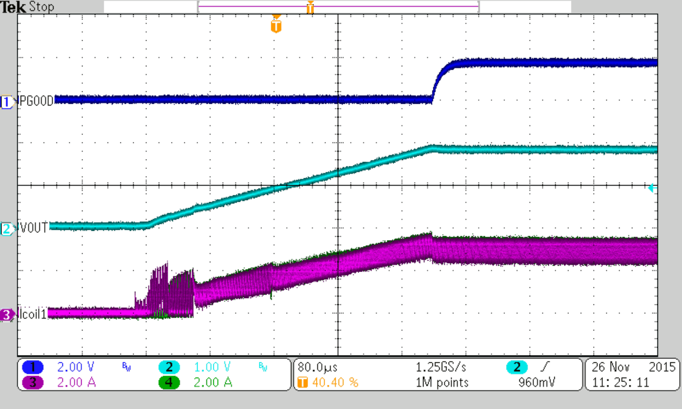
TPSM82480 SLVSCL9_stuplow.gif
VOUT = 1.8 V
Figure 24. Startup into 3.3 Ω resistor
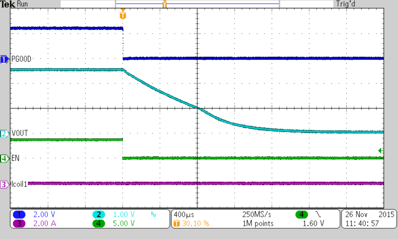
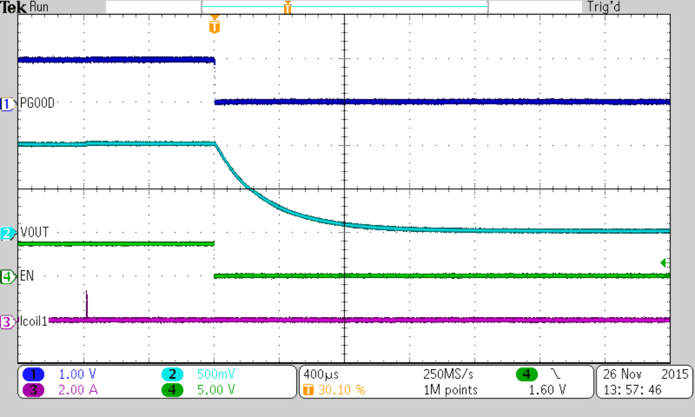
TPSM82480 SLVSCL9_discharge2.5V.gif
VOUT = 2.5 V no load
Figure 26. Output Discharge
TPSM82480 SLVSCL9_PWMtyp.gif
Figure 28. Typical Operation PWM
TPSM82480 SLVSCL9_ADD2nd.gif
Figure 30. Adding 2nd Phase
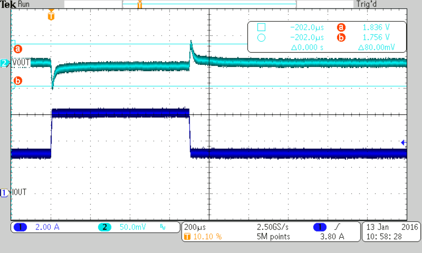
TPSM82480 SLVSCL9_tran_0-3.gif
Figure 32. Load Transient Response (PSM-PWM),
Load Step 0 to 3 A
TPSM82480 SLVSCL9_tran_3-6.gif
Figure 34. Load Transient Response (PWM-PWM),
Load Step 3 to 6 A
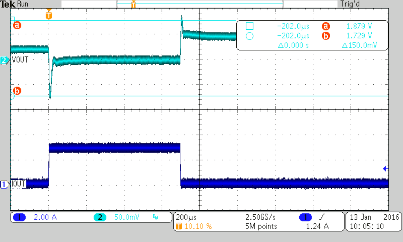
TPSM82480 SLVSCL9_tran_0-6cff.gif
Cff = 36 pF (nom)
Figure 36. Load Transient Response (PWM-PWM),
Load Step 0 to 6 A
TPSM82480 SLVSDT1_SOA33.gif
VIN = 5 V VOUT = 3.3 V
Figure 38. Maximum Ambient Temperature for TJ=125°C
(TPSM82480 EVM)
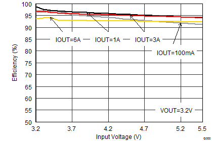
TPSM82480 SLVSDT1_eff32_vin.gif
VOUT = 3.2 V
Figure 11. Efficiency vs Input Voltage
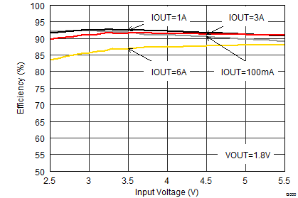
TPSM82480 SLVSDT1_eff18_vin.gif
VOUT = 1.8 V
Figure 13. Efficiency vs Input Voltage
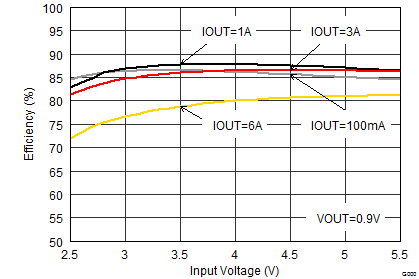
TPSM82480 SLVSDT1_eff09_vin.gif
VOUT = 0.9 V
Figure 15. Efficiency vs Input Voltage
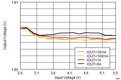
TPSM82480 SLVSCL9_linereg.gif
MODE = High
Figure 17. Output Voltage vs Input Voltage
(Line Regulation)
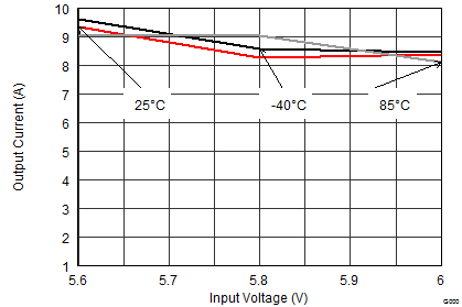
TPSM82480 SLVSCL9_IOUTmax_5.5V.gif
VOUT = 5.5 V
Figure 19. Maximum Output Current
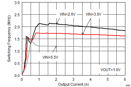
TPSM82480 SLVSCL9_FSWiout1.0V_lin.gif
VOUT = 1 V
Figure 21. Switching Frequency vs Output Current
TPSM82480 VSEL High EMI.gif
VIN = 6 V (battery supply) RLOAD = 0.47 Ω VOUT = 2.5 V
EMI test board without filters VSEL High
Figure 23. TPSM82480 Radiated Emissioins
TPSM82480 SLVSCL9_stuphigh.gif
VOUT = 1.8 V
Figure 25. Startup into 0.3 Ω resistor
TPSM82480 SLVSCL9_discharge1.0V.gif
VOUT = 1 V no load
Figure 27. Output Discharge
TPSM82480 SLVSCL9_PSMtyp.gif
IOUT = 50 mA
Figure 29. Typical Operation PSM
TPSM82480 SLVSCL9_SHED2nd.gif
Figure 31. Shedding 2nd Phase
TPSM82480 SLVSCL9_tran_0-3cff.gif
Cff = 36 pF (nom)
Figure 33. Load Transient Response (PSM-PWM),
Load Step 0 to 3 A
TPSM82480 SLVSCL9_tran_3-6cff.gif
Cff = 36 pF (nom)
Figure 35. Load Transient Response (PWM-PWM),
Load Step 3 to 6 A
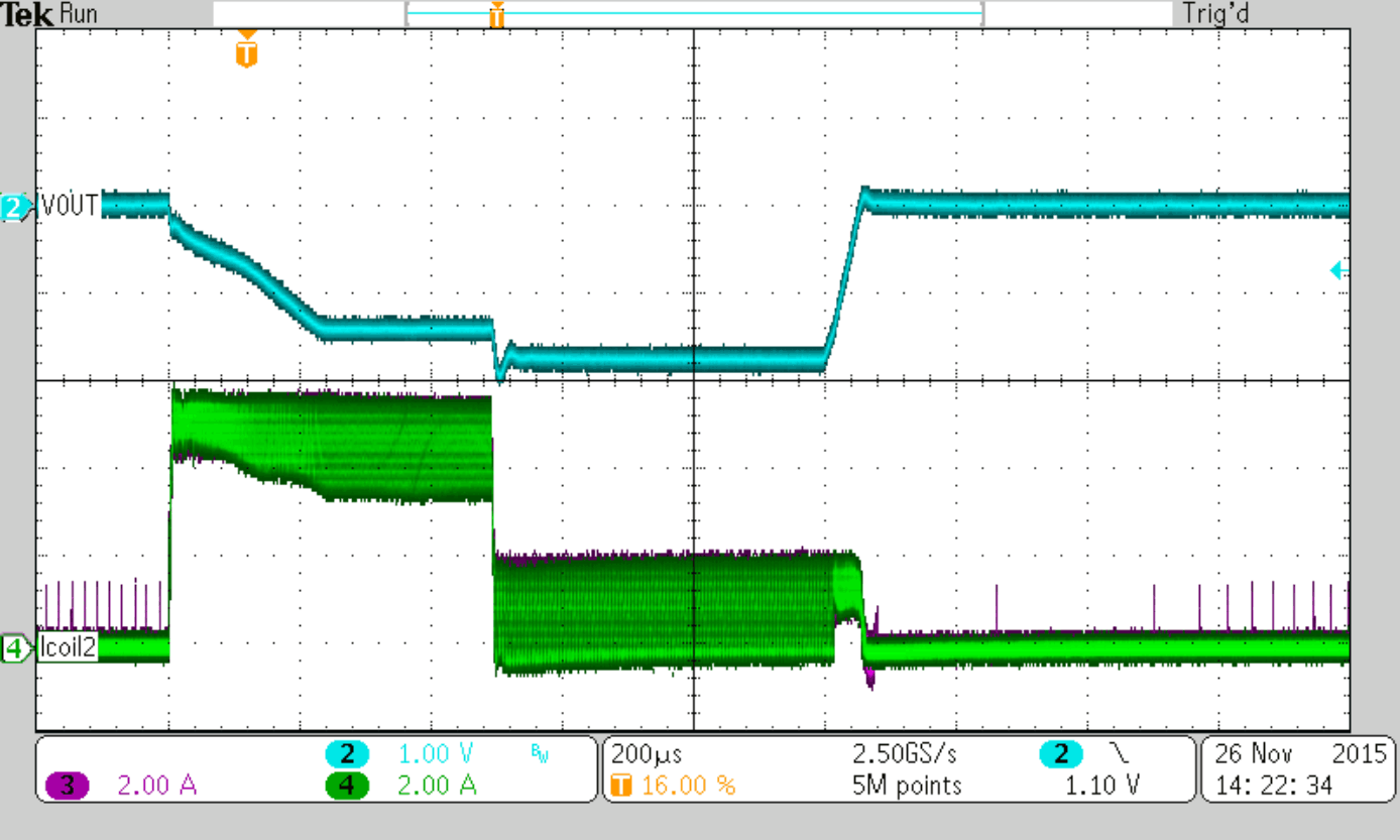
TPSM82480 SLVSCL9_climfoldback.gif
IOUT = 10 A
Figure 37. Current Limit Fold-Back at Overload
TPSM82480 SLVSDT1_thermal33.gif
VIN = 5 V VOUT = 3.3 V IOUT = 6 A
Figure 39. Device Temperature (TPSM82480 EVM)